System-level packaging method and packaging structure
A system-level packaging and PCB board technology, which is applied in the manufacture of electrical components, electrical solid devices, semiconductor/solid devices, etc., can solve the problems of large thickness and incompatible with the thinning of portable products, and reduce the bonding stress , Enhance the efficiency of electrical connection and simplify the packaging process
- Summary
- Abstract
- Description
- Claims
- Application Information
AI Technical Summary
Problems solved by technology
Method used
Image

Examples
Embodiment 1
[0030] The present invention provides a system-level packaging method, comprising the following steps:
[0031] S01. Provide a PCB board, on which a plurality of exposed first pads are formed;
[0032] S02. Provide a first device wafer, on which a first chip is formed, and the first chip has a plurality of exposed second pads;
[0033] S03, bonding the first device wafer to the PCB board, the first welding pad and the second welding pad are arranged oppositely to form a gap;
[0034] S04, using an electroplating process to form a conductive bump in the gap, and the first pad and the second pad are electrically connected through the conductive bump.
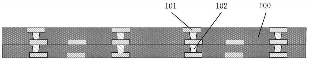
[0035] Figure 1-Figure 7 It is a structural diagram corresponding to each step of the system-in-package method in this embodiment. Please refer below Figure 1-Figure 7 The system-in-package method is described.
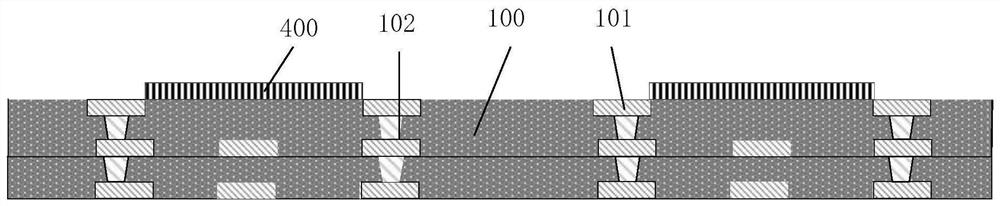
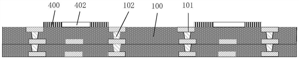
[0036] Please refer to figure 1 , step S01 is executed to provide a PCB board 100 on which a plurality of expose...
Embodiment 2
[0072] refer to Figure 8 This embodiment 2 provides a structural schematic diagram of another packaging method. The difference between this embodiment 2 and embodiment 1 is that after the conductive bumps 301 are formed, the PCB board 100 includes opposite front and back sides, and the first solder joint is formed. One side of the pad 101 is the front side of the PCB board 100, and the second device wafer 500 is bonded to the back side of the PCB board 100, and a second chip 501 is formed on the second device wafer 500, and the PCB board 100 and the second device wafer 500 Conductive bumps 301 or solder balls are electrically connected to each other by an electroplating process.
[0073]In this embodiment, the second device wafer 500 or other chips are bonded on the back of the PCB board 100 , and the second device wafer 500 is taken as an example for description in this embodiment. Form the exposed third welding pad 103 on the back side of the PCB board 100, form the second...
Embodiment 3
[0080] refer to Figure 9 , Embodiment 3 provides a schematic structural diagram of another packaging method. The difference between Embodiment 3 and Embodiment 1 and Embodiment 2 is that after the conductive bumps 301 are formed, the first device wafer 200 includes an opposite front and the back side, the side where the second bonding pad 202 is formed is the front side of the first device wafer 200, and the third device wafer 600 is bonded to the back side of the first device wafer 200, the third device wafer is formed with a third chip, Conductive bumps 301 or solder balls are electrically connected between the first device wafer 200 and the third chip 601 on the third device wafer 600 through an electroplating process.
[0081] In this embodiment, the third device wafer 600 or other chips are bonded on the backside of the first device wafer 200 , and the third device wafer 600 is taken as an example for description in this embodiment. On the back side of the first device ...
PUM
| Property | Measurement | Unit |
|---|---|---|
| Thickness | aaaaa | aaaaa |
| Thickness | aaaaa | aaaaa |
| Height | aaaaa | aaaaa |
Abstract
Description
Claims
Application Information
 - Generate Ideas
- Intellectual Property
- Life Sciences
- Materials
- Tech Scout
- Unparalleled Data Quality
- Higher Quality Content
- 60% Fewer Hallucinations
Browse by: Latest US Patents, China's latest patents, Technical Efficacy Thesaurus, Application Domain, Technology Topic, Popular Technical Reports.
© 2025 PatSnap. All rights reserved.Legal|Privacy policy|Modern Slavery Act Transparency Statement|Sitemap|About US| Contact US: help@patsnap.com