Semiconductor structure and forming method thereof

A semiconductor and gate structure technology, applied in the field of semiconductor structure and its formation, can solve the problems of semiconductor structure performance to be improved, and achieve the effects of improving electrical connection performance, reducing power consumption, and improving delay

Pending Publication Date: 2022-07-26
SEMICON MFG INT (SHANGHAI) CORP +1
View PDF0 Cites 0 Cited by
  • Summary
  • Abstract
  • Description
  • Claims
  • Application Information

AI Technical Summary

Problems solved by technology

[0005] However, the performance of current semiconductor structures still needs to be improved

Method used


Image

  • Semiconductor structure and forming method thereof
  • Semiconductor structure and forming method thereof
  • Semiconductor structure and forming method thereof

Examples


Embodiment Construction

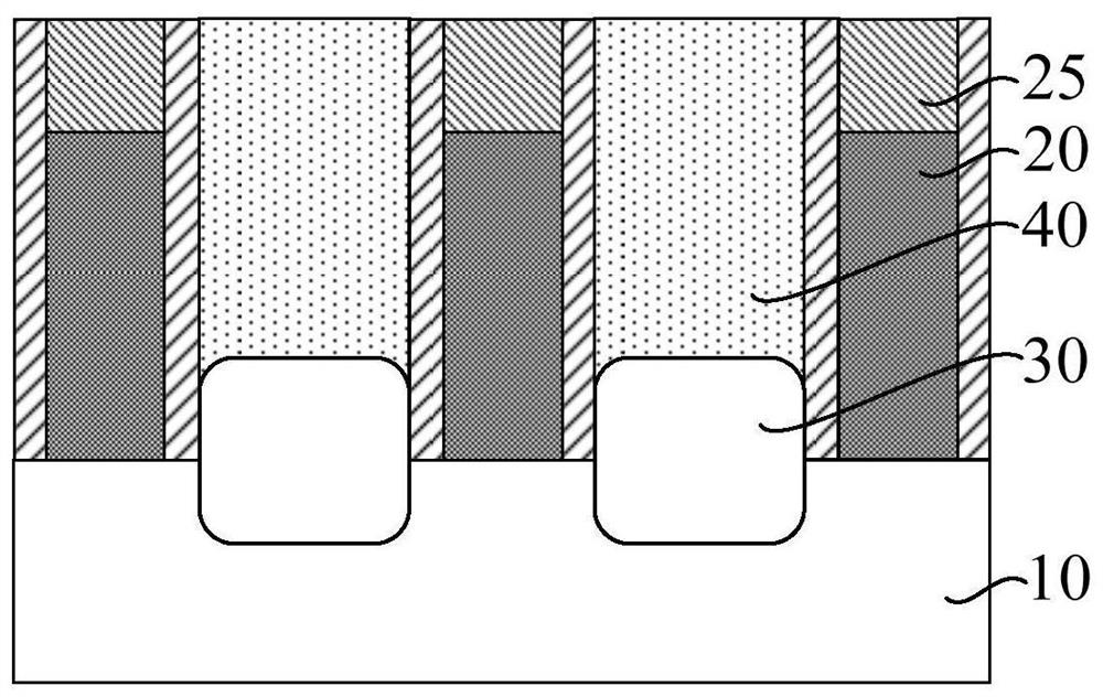
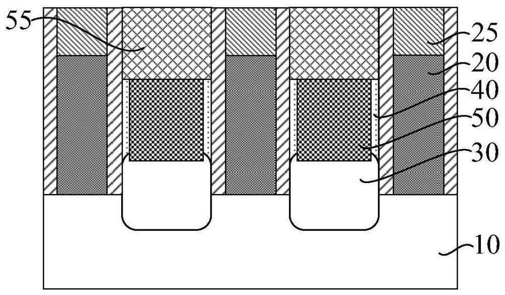
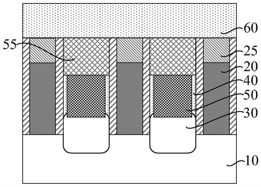
[0017] It can be known from the background art that the performance of the current semiconductor structure needs to be improved. The reason why the performance of the semiconductor structure needs to be improved is now analyzed in combination with a method for forming a semiconductor structure. Figure 1 to Figure 6 It is a schematic structural diagram corresponding to each step in a method for forming a semiconductor structure.

[0018] refer to figure 1 , a substrate 10 is provided, a gate structure 20 is formed on the substrate 10, a gate capping layer 25 is formed on the top surface of the gate structure 20, and source and drain doped regions are formed in the substrate 10 on both sides of the gate structure 20 30 , a bottom dielectric layer 40 covering the source and drain doped regions 30 is formed on the substrate 10 on the side of the gate structure 20 , and the bottom dielectric layer 40 exposes the top surface of the gate capping layer 25 .

[0019] refer to figu...


PUM

PropertyMeasurementUnit
thicknessaaaaaaaaaa
thicknessaaaaaaaaaa

Abstract

The invention discloses a semiconductor structure and a forming method thereof. The semiconductor structure comprises a substrate; the gate structure is separated from the substrate and comprises a gate contact region which is in contact with the gate plug; the source-drain doped region comprises a source-drain contact region and a source-drain connection region; the dielectric structure layer is positioned on the substrate at the side part of the gate structure and covers the source-drain doped region and the gate structure; the source-drain contact structure is in contact with the source-drain doped region, the source-drain contact structure is of an integrated structure and comprises a source-drain plug penetrating through the dielectric structure layer of the source-drain contact region and a source-drain contact layer located in the dielectric structure of the source-drain connection region, and the top surface of the source-drain contact layer is lower than the top surface of the source-drain plug; the source-drain contact structure and the dielectric structure layer enclose an interval opening; the interval dielectric layer is filled in the interval opening; and the gate plug is positioned at the top of the gate structure of the gate contact region and is in contact with the gate structure. According to the embodiment of the invention, the source-drain contact structure is an integrated structure, and the electrical connection performance between the source-drain plug and the source-drain contact layer is improved.

Description

technical field [0001] Embodiments of the present invention relate to the field of semiconductor manufacturing, and in particular, to a semiconductor structure and a method for forming the same. Background technique [0002] With the continuous development of integrated circuit manufacturing technology, people's requirements for the integration and performance of integrated circuits are becoming higher and higher. In order to improve the integration level and reduce the cost, the critical dimensions of the components are becoming smaller, and the circuit density inside the integrated circuit is increasing. This development makes the wafer surface unable to provide enough area to make the required interconnection lines. [0003] In order to meet the requirements of interconnect lines after the critical dimension has been shrunk, the current conduction between different metal layers or the metal layers and the substrate is achieved through an interconnect structure. The inter...

Claims


Application Information

Patent Timeline
Patent Type & Authority Applications(China)
IPC IPC(8): H01L27/088H01L21/8234
CPCH01L27/088H01L21/823475H01L21/823418H01L21/823437H01L29/41791H01L29/66795H01L29/401H01L29/41775
Inventor 王楠
Owner SEMICON MFG INT (SHANGHAI) CORP
Why Eureka
Try Eureka