Method for regulating and controlling longitudinal morphology of organic solar cell through solvent annealing post-treatment
A technology of solar cells and organic electronics, applied in circuits, photovoltaic power generation, electrical components, etc., can solve the problem that there is no reasonable and universal method for the regulation of the longitudinal morphology of the active layer, and the research on the regulation of solar cell morphology is not comprehensive enough, etc. The problem is to achieve the effect of simple and feasible preparation method, vertical improvement and efficiency improvement.
- Summary
- Abstract
- Description
- Claims
- Application Information
AI Technical Summary
Problems solved by technology
Method used
Image
Examples
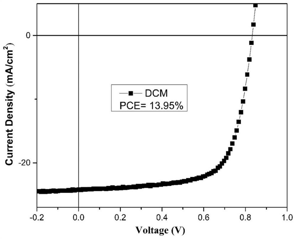
Embodiment 1
[0046] Fine tuning of the longitudinal morphology of the active layer by DCM solvent vapor annealing
[0047] 1. Cleaning of ITO conductive glass: The ITO substrate was repeatedly ultrasonically cleaned with deionized water for 4 times for 15 minutes, and isopropanol for 30 minutes respectively. After cleaning, it was placed in a drying oven at 70 °C for drying and preservation.
[0048] 2. Preparation of anode transport layer: The purchased PEDOT:PSS (4083) was spin-coated on an ITO substrate at 3000 rpm, and then baked at a high temperature of 150° C. for 15 minutes, with a thickness of about 40 nm.
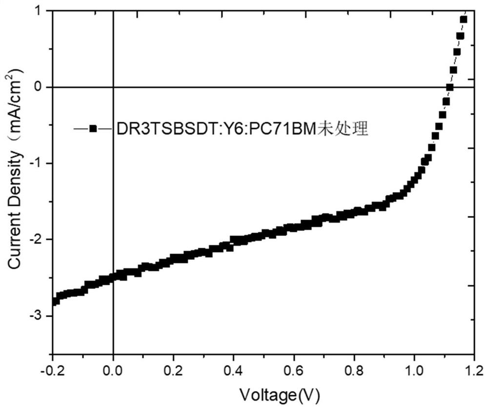
[0049] 3. Preparation of the organic photoactive layer: the mass ratio of the donor and the acceptor DR3TSBSDT:Y6:PC71BM is 1.25:0.6:0.4, and the concentration of the mixed solution of the donor and the acceptor is 18 mg / mL; The bulk mixed solution uses an organic solvent as the main solvent CF to prepare a photoactive layer with a thickness of about 120 nm.
[0050] 4. Post-t...
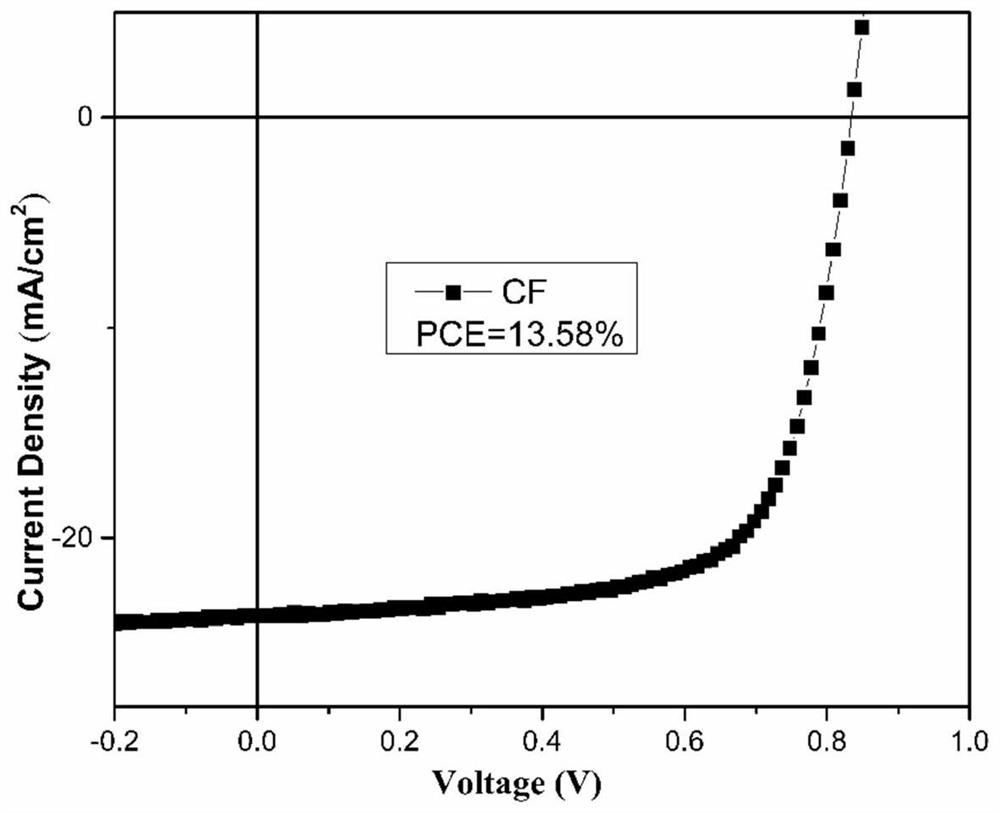
Embodiment 2
[0055] Fine tuning of the longitudinal morphology of the active layer by CF solvent vapor annealing
[0056] 1. Cleaning of ITO conductive glass: The ITO substrate was repeatedly ultrasonically cleaned with deionized water for 4 times for 15 minutes, and isopropanol for 30 minutes respectively. After cleaning, it was placed in a drying oven at 70 °C for drying and preservation.
[0057] 2. Preparation of anode transport layer: The purchased PEDOT:PSS (4083) was spin-coated on an ITO substrate at 3000 rpm, and then baked at a high temperature of 150° C. for 15 minutes, with a thickness of about 40 nm.
[0058] 3. Preparation of the organic photoactive layer: the mass ratio of the donor and the acceptor DR3TSBSDT:Y6:PC71BM is 1.25:0.6:0.4, and the concentration of the mixed solution of the donor and the acceptor is 18 mg / mL; The bulk mixed solution uses an organic solvent as the main solvent CF to prepare a photoactive layer with a thickness of about 120 nm.
[0059] 4. Post-tr...
example 1
[0065] The structural formulas of the fullerene acceptors in Examples 1 and 2 are shown below:
[0066]
[0067] The structural formulas of the small molecule receptors in Examples 1 and 2 are shown below:
[0068]
PUM
| Property | Measurement | Unit |
|---|---|---|
| thickness | aaaaa | aaaaa |
| thickness | aaaaa | aaaaa |
| thickness | aaaaa | aaaaa |
Abstract
Description
Claims
Application Information
 - R&D Engineer
- R&D Manager
- IP Professional
- Industry Leading Data Capabilities
- Powerful AI technology
- Patent DNA Extraction
Browse by: Latest US Patents, China's latest patents, Technical Efficacy Thesaurus, Application Domain, Technology Topic, Popular Technical Reports.
© 2024 PatSnap. All rights reserved.Legal|Privacy policy|Modern Slavery Act Transparency Statement|Sitemap|About US| Contact US: help@patsnap.com


