Field effect transistor device based on two-dimensional interlayer slippage ferroelectric semiconductor and preparation method thereof

A field effect transistor, interlayer slip technology, applied in semiconductor/solid state device manufacturing, semiconductor devices, electrical components, etc., can solve the problems of no longer providing performance improvement, increasing manufacturing costs, etc., to achieve voltage reduction, low power consumption Effects of storage, shrinking device size

Active Publication Date: 2022-07-05
UNIV OF ELECTRONICS SCI & TECH OF CHINA
View PDF12 Cites 2 Cited by
  • Summary
  • Abstract
  • Description
  • Claims
  • Application Information

AI Technical Summary

Problems solved by technology

With the end of Moore's Law, the increase in manufacturing costs and the limitations of the underlying

Method used


Image

  • Field effect transistor device based on two-dimensional interlayer slippage ferroelectric semiconductor and preparation method thereof
  • Field effect transistor device based on two-dimensional interlayer slippage ferroelectric semiconductor and preparation method thereof
  • Field effect transistor device based on two-dimensional interlayer slippage ferroelectric semiconductor and preparation method thereof

Examples


Embodiment Construction

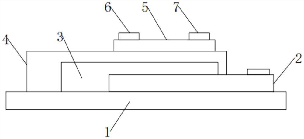
[0022] A field effect transistor device based on a two-dimensional interlayer slip ferroelectric semiconductor and a preparation method thereof of the present invention will be further described with reference to the accompanying drawings.

[0023] A field effect transistor device based on a two-dimensional interlayer slip ferroelectric semiconductor of the present invention includes a supporting substrate 1, a back gate electrode 2, a ferroelectric dielectric layer 3, an insulating dielectric layer 4 and a source that are sequentially stacked from bottom to top Drain electrode, the source-drain electrode includes a source electrode 6 and a drain electrode 7, a conductive channel 5 is provided between the source electrode 6 and the drain electrode 7, and the conductive channel 5 is a graphene material, The ferroelectric dielectric layer 3 is a layered two-dimensional interlayer slip ferroelectric semiconductor material GaSe, the insulating dielectric layer 4 is a h-BN material,...


PUM


Abstract

According to the III-VI group material (GaSe)-based interlayer slippage ferroelectric field effect transistor device, the characteristic that interlayer slippage is controlled by an electric field in the material to achieve polarization overturning is utilized, regulation and control over the Fermi level and the conductivity of a channel can be achieved, and compared with a traditional ferroelectric field effect transistor, the device has the advantages that the device is simple in structure and convenient to implement. According to the two-dimensional ultrathin ferroelectric, the size of the device can be remarkably reduced, an effective gate electric field is increased, and the voltage required by overturning or polarization can be further reduced, so that low-power-consumption storage can be realized. The novel ferroelectric field effect transistor device for regulating and controlling interlayer slippage by the external electric field provides a new platform for realizing high-performance ferroelectric storage and a high-integration-level storage chip.

Description

Technical field: [0001] The invention relates to the technical field of semiconductors, in particular to a field effect transistor device based on a two-dimensional interlayer slip ferroelectric semiconductor and a preparation method thereof. Background technique: [0002] In today's big data era, in the face of urgent high-performance computing needs, especially when dealing with complex real-time pattern recognition and natural language processing programs, the performance of the current Von Neumann system is difficult to match the average human. Brain level matching. Device shrinkage can drive increased computing power, while device size reductions allow for improvements in speed and power. With the end of Moore's theorem, increased manufacturing costs and limitations in underlying physics mean that device shrinking by itself can no longer provide the desired performance improvements. Therefore, innovative devices have become particularly important to meet our strong de...

Claims


Application Information

Patent Timeline
IPC IPC(8): H01L29/423H01L29/10H01L29/16H01L29/78H01L21/336
CPCH01L29/42364H01L29/1033H01L29/1606H01L29/78391H01L29/6684Y02P70/50
Inventor 刘富才马博文卞仁吉
Owner UNIV OF ELECTRONICS SCI & TECH OF CHINA
Why Eureka
Try Eureka