
Display backboard, manufacturing method thereof and display device

A technology for display backplanes and substrate substrates, which is applied in the manufacture of semiconductor/solid-state devices, semiconductor devices, electrical components, etc., and can solve the problems of large pressure drop of the second electrode.

Pending Publication Date: 2022-07-05
HEFEI XINSHENG OPTOELECTRONICS TECH CO LTD +1
View PDF0 Cites 2 Cited by
  • Summary
  • Abstract
  • Description
  • Claims
  • Application Information

AI Technical Summary

Problems solved by technology

Therefore, an object of the present invention is to provide a display backplane, which can well solve the problem of large voltage drop of the second electrode layer, or improve the stability of the structure of the first electrode layer in the light emitting structure

Method used


Image

  • Display backboard, manufacturing method thereof and display device
  • Display backboard, manufacturing method thereof and display device
  • Display backboard, manufacturing method thereof and display device

Examples


Embodiment Construction

[0019] The solution of the present invention will be explained below in conjunction with the embodiments. Those skilled in the art will understand that the following examples are only used to illustrate the present invention, and should not be construed as limiting the scope of the present invention. If no specific technique or condition is indicated in the examples, the technique or condition described in the literature in the field or the product specification is used.

[0020] The present invention will be described below with reference to specific embodiments. It should be noted that these embodiments are only illustrative and do not limit the present invention in any way.

[0021] In one aspect of the present invention, the present invention provides a display backplane. According to an embodiment of the present invention, refer to figure 1 , the display backplane includes: a base substrate, and a light-emitting structure, a pixel definition layer 40 and an isolation st...


PUM


Abstract

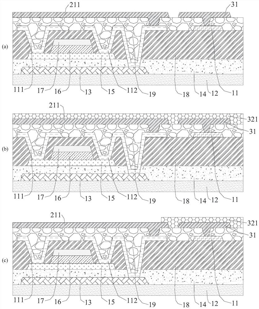
The invention provides a display backboard, a manufacturing method thereof and a display device. In the display backboard, a light-emitting structure comprises a first electrode layer, a light-emitting layer and a second electrode layer, at least part of the light-emitting structure is located in an opening of a pixel definition layer, and the first electrode layer is arranged close to a substrate; the isolation structure is located on the side, away from the opening, of the pixel definition layer; one part of the second electrode layer extends to the side surface, close to the pixel definition layer, of the isolation structure from the opening of the pixel definition layer along the pixel definition layer through a gap between the pixel definition layer and the isolation structure, and the second electrode layer is electrically connected to the isolation structure; the light-emitting layer is not connected at the gap between the pixel definition layer and the isolation structure; in the direction perpendicular to the substrate, the height of the isolation structure is larger than that of the first electrode layer. The thickness of the first electrode layer is small, the problem that a metal film layer of the reflection first electrode layer swells or falls off can be smoothly solved, and then the display effect and the product yield of the product are remarkably improved.

Description

technical field [0001] The present invention relates to the field of display technology, and in particular, to a display backplane, a manufacturing method thereof, and a display device. Background technique [0002] Transparent display products are widely used in in-vehicle displays such as automobiles / subways and window displays in hotels / clothing stores. Large-scale transparent display products will make the cathode very thin in order to improve the transparent effect, but this will lead to the problem of large IR drop (voltage drop) of the cathode. An effective solution is to connect the cathode with the conductive structure on the backplane. Effectively overlap, thereby greatly reducing the IR drop problem. The current effective lap joint method is to prepare an "I"-shaped Rib structure on the backplane, so that the protruding Tip corner on the upper end can smoothly cut off the vapor-deposited EL luminescent material, and then the cathode can be deposited in and smooth...

Claims


Application Information

Patent Timeline
IPC IPC(8): H01L27/32H01L21/77
CPCH10K59/122H10K59/131H10K59/1201
Inventor 刘宁周斌刘军闫梁臣
Owner HEFEI XINSHENG OPTOELECTRONICS TECH CO LTD
Learn More