Antimonide semiconductor device and preparation method thereof

An antimonide and semiconductor technology, applied in the field of antimonide semiconductor devices and their preparation, can solve the problems of reversed-phase domain defects, poor compatibility between an antimonide epitaxial layer and a silicon substrate, etc., achieve high crystal quality, and alleviate lattice mismatch. Stress, cost reduction effect

Pending Publication Date: 2022-06-28
埃特曼(北京)半导体技术有限公司
View PDF0 Cites 0 Cited by
  • Summary
  • Abstract
  • Description
  • Claims
  • Application Information

AI Technical Summary

Problems solved by technology

[0005] The purpose of the present invention is to provide an antimonide semiconductor device and its preparation method to solve the problems of poor compatibility between the antimonide epitaxial layer and the silicon substrate and serious antiphase domain defects in the prior art

Method used


Image

  • Antimonide semiconductor device and preparation method thereof
  • Antimonide semiconductor device and preparation method thereof
  • Antimonide semiconductor device and preparation method thereof

Examples


specific Embodiment approach 3

[0050] The present invention also provides a method for preparing an antimonide semiconductor device, and a schematic flow diagram of a specific embodiment thereof is as follows: Figure 5 As shown, it is called specific embodiment three, including:

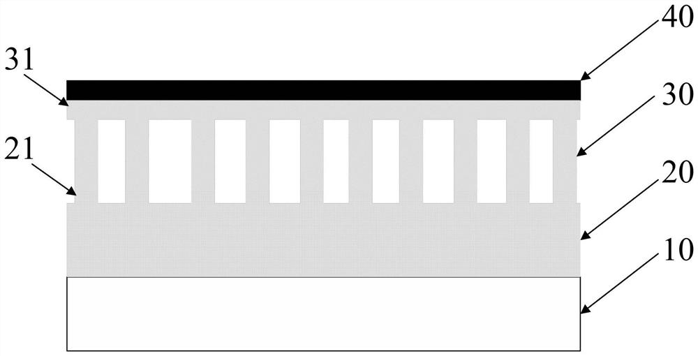
[0051] S101 : growing a lattice transition buffer layer on the silicon-based substrate 10 .

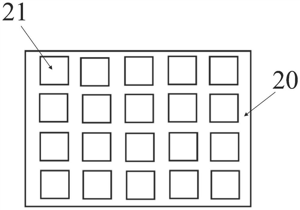
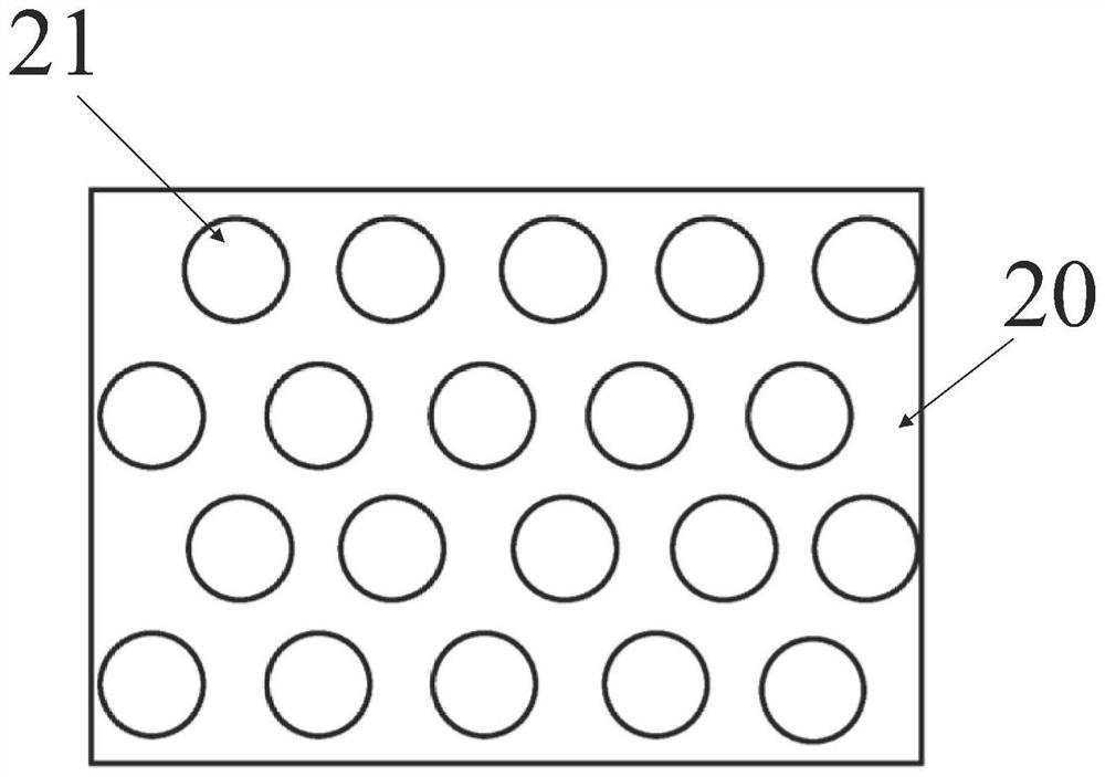
[0052] S102 : Perform patterning processing on the lattice transition buffer layer to obtain a patterned buffer layer 20 including a plurality of raised bases 21 .

[0053] S103 : growing a columnar structure on the patterned buffer layer 20 to obtain a three-dimensional columnar buffer layer 30 ; wherein the tops of the three-dimensional columnar buffer layer 30 are connected to each other to form a two-dimensional crystal plane 31 .

[0054] S104 : growing an antimonide structure layer 40 on the two-dimensional crystal plane 31 to obtain the antimonide semiconductor device.

[0055] The antimonide structure layer 40 may be the conven...


PUM

PropertyMeasurementUnit
thicknessaaaaaaaaaa
thicknessaaaaaaaaaa
thicknessaaaaaaaaaa

Abstract

The invention relates to the field of semiconductor manufacturing, and particularly discloses an antimonide semiconductor device and a preparation method thereof, and the antimonide semiconductor device sequentially comprises a silicon-based substrate, a graphical buffer layer, a three-dimensional columnar buffer layer and an antimonide structure layer from bottom to top. The graphical buffer layer comprises raised bases which are arranged in a graphical manner, and the columnar structure of the three-dimensional columnar buffer layer grows depending on the raised bases; the columnar structures are mutually connected at the top of the three-dimensional columnar buffer layer to form a two-dimensional crystal surface, and the antimonide structure layer grows on the two-dimensional crystal surface. The two-dimensional crystal surface is provided with regular protrusions and recesses, lattice mismatch stress and thermal stress can be effectively relieved, the anti-phase domain defect problem of antimonide growing on a silicon-based substrate is relieved, an antimonide semiconductor device with high active area crystal quality is obtained, the buffer layer is simple in structural component, growth can be completed in MOCVD, and the production cost is low. The MBE growth method does not need high-precision control, and the cost is reduced.

Description

technical field [0001] The invention relates to the field of semiconductor manufacturing, in particular to an antimonide semiconductor device and a preparation method thereof. Background technique [0002] Antimonide semiconductors are semiconductor materials whose lattice constants are concentrated around 6.1 angstroms. Due to the diverse band gap distributions, antimonides can form various heterostructures and are used in different fields such as optoelectronics and radio frequency. In the epitaxial link of antimonide infrared lasers, detectors, high electron mobility transistors and other structures, InSb, GaSb or InP substrates with lattice constants that match the antimonide epitaxial structure are generally selected, but the above substrates are generally expensive. The problem of poor stability. [0003] At present, the silicon substrate with mature integrated technology is cheap, but there is a large lattice mismatch between antimonide and antimonide, and the growth...

Claims


Application Information

Patent Timeline
Patent Type & Authority Applications(China)
IPC IPC(8): H01L29/06H01L31/0352H01L31/18H01L21/02H01S5/028H01S5/30
CPCH01L29/0684H01L29/0657H01L31/035281H01L31/035272H01L31/18H01S5/30H01S5/3013H01L21/02381H01L21/02513H01L21/02502H01L21/02549H01S5/028H01S2304/00
Inventor 董海云倪健薛聪
Owner 埃特曼(北京)半导体技术有限公司
Why Eureka
Try Eureka