Formation method of semiconductor structure

A semiconductor and isolation structure technology, applied in the field of semiconductor structure formation, can solve problems such as poor performance of semiconductor structures, and achieve the effects of performance improvement, reduction of dummy gate structure residues, and performance improvement

Pending Publication Date: 2022-06-28
SEMICON MFG INT (SHANGHAI) CORP +1
View PDF0 Cites 0 Cited by
  • Summary
  • Abstract
  • Description
  • Claims
  • Application Information

AI Technical Summary

Problems solved by technology

[0004] However, the performance of the semiconductor structure formed by the gate cut-off process in the prior art is poor

Method used


Image

  • Formation method of semiconductor structure
  • Formation method of semiconductor structure
  • Formation method of semiconductor structure

Examples


Embodiment Construction

[0030] As described in the background art, the semiconductor structures formed by the gate cut-off process in the prior art have poor performance. The following will be described in detail with reference to the accompanying drawings.

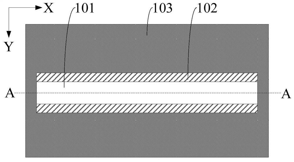
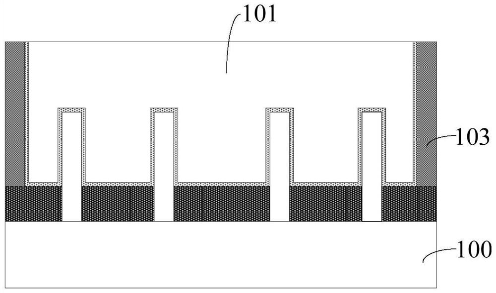
[0031] Please refer to figure 1 and figure 2 , figure 2 Yes figure 1 A schematic cross-sectional view along the line A-A in the middle, a substrate 100 is provided; an initial dummy gate structure 101 is formed on the substrate 100 , and the initial dummy gate structure 101 extends along the first direction X; on the side of the initial dummy gate structure 101 forming a spacer 102 on the wall; forming a dielectric layer 103 on the substrate 100, the dielectric layer 103 covering the initial dummy gate structure 101 and the spacer 102, and the dielectric layer 103 exposing the initial The top surface of the dummy gate structure 102 and the spacers 103 .

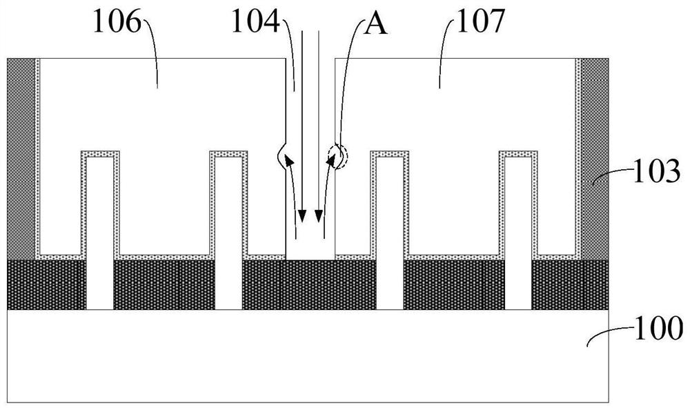
[0032] Please refer to image 3 , image 3 and figure 2 The view direction is ...


PUM


Abstract

A method for forming a semiconductor structure comprises the steps that a substrate is provided, and the substrate comprises a base and a plurality of fin parts which are located on the base and are separated from one another; forming a pseudo gate structure on the substrate, wherein the pseudo gate structure comprises a first region and a second region located on the first region; removing a part of the second region, and forming a first opening in the pseudo gate structure; forming a passivation layer on the side wall of the first opening; and removing the first region exposed by the first opening, and forming a second opening in the pseudo gate structure. Due to the existence of the passivation layer, the damage of the etching gas to the passivation layer is small, and the problem that the side wall of the first opening is sunken is reduced, so that the pseudo gate structure is relatively completely removed subsequently, the performance of the gate structure formed subsequently is improved, and the performance of the finally formed semiconductor structure is improved.

Description

technical field [0001] The present invention relates to the technical field of semiconductor manufacturing, and in particular, to a method for forming a semiconductor structure. Background technique [0002] With the continuous development of semiconductor technology, the improvement of integrated circuit performance is mainly achieved by continuously reducing the size of integrated circuit devices to increase its speed. Currently, as the semiconductor industry has advanced to nanotechnology process nodes in pursuit of high device density, high performance, and low cost, the fabrication of semiconductor devices is limited by various physical limits. [0003] In the manufacturing process of the integrated circuit, the strip-shaped gate needs to be cut off by a gate cut (Poly Cut) process. After cutting, the gate corresponds to different transistors, which can improve the integration degree of the transistors. In addition, when a plurality of gates are arranged in a row along...

Claims


Application Information

Patent Timeline
IPC IPC(8): H01L21/336H01L29/78H01L29/423
CPCH01L29/66803H01L29/785H01L29/42356
Inventor 赵琼洋毕晓峰朱建校
Owner SEMICON MFG INT (SHANGHAI) CORP
Why Eureka
Try Eureka