PCBA needle bed testing machine and testing method

A testing machine and needle bed technology, applied in the field of semiconductor testing equipment, can solve the problems that the processing cycle cannot meet the needs of production, increase processing costs, and high density of test points, reduce the number of test points and processing difficulty, improve the safety factor, The effect of improving economic efficiency

Inactive Publication Date: 2022-06-28
NANJING MACROTEST SEMICON TECH CO LTD
View PDF6 Cites 0 Cited by
  • Summary
  • Abstract
  • Description
  • Claims
  • Application Information

AI Technical Summary

Problems solved by technology

[0002] The current PCBA design is becoming more and more complicated, and the board density is getting higher and higher. In order to test the integrity of the signal, more and more test point signals are required, which increases the difficulty of PCBA design.
[0003] At present, the semiconductor testing equipment that uses the bed of needles test can only move in one dimension to complete the test. As a result, when the test point density of the tested board is high, the processing accuracy of the needle bed of the test equipment is getting higher and higher. The processing cycle will become increasingly unable to meet the needs of production
Moreover, the density of test points is too high, which will make processing difficult, easily increase the defective rate, and increase processing costs
[0004] During use, when the test points are too dense, there is a risk of short circuit caused by contact between thimbles

Method used


Image

  • PCBA needle bed testing machine and testing method
  • PCBA needle bed testing machine and testing method

Examples


Embodiment Construction

[0021] The technical solutions in the embodiments of the present invention will be clearly and completely described below with reference to the accompanying drawings in the embodiments of the present invention; obviously, the described embodiments are only a part of the embodiments of the present invention, not all of the embodiments. The embodiments of the present invention, and all other embodiments obtained by those of ordinary skill in the art without creative work, fall within the protection scope of the present invention.

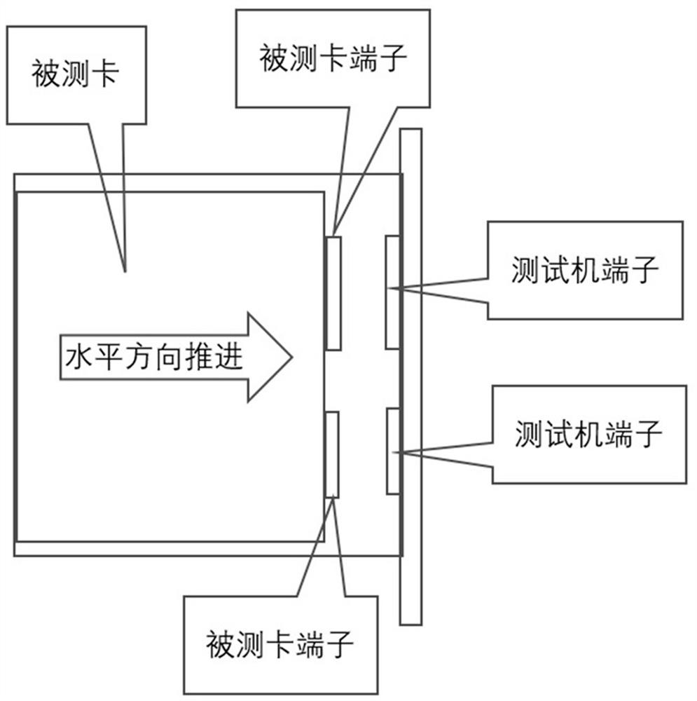
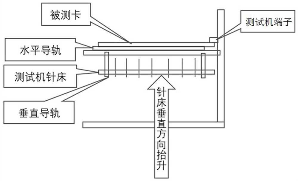
[0022] The general test device can only move in one dimension. For the card under test with relatively dense test points, it increases the difficulty of positioning and processing the thimble of the test device, which is likely to cause a defective rate and increase the processing cost.

[0023] For a specific card under test, its area is limited, and test points cannot be added unlimitedly.

[0024] In the actual test, when the thimbles are too dense...


PUM


Abstract

The invention provides a PCBA needle bed testing machine and a testing method, and the testing method proposes the feasibility of leading out a part of testing signals to a testing device in other dimensions by reducing the density or number of testing points in a single dimension. According to the PCBA needle bed testing machine provided by the invention, the testing machine comprises a horizontal testing assembly and a vertical testing assembly, the horizontal testing assembly is used for testing a tested card in the horizontal dimension by the testing machine, and the vertical testing assembly is used for testing the tested card in the vertical dimension by the testing machine. According to the invention, the existing tested card terminal on the board card is used as a test interface of another dimension, so that additional test points are not needed when the PCB is designed, and the number of the test points of the needle bed of the test equipment and the processing difficulty are reduced. The technical scheme is low in cost, high in safety coefficient, rapid and efficient.

Description

technical field [0001] The invention belongs to the technical field of semiconductor testing equipment, and in particular relates to a PCBA bed of needles testing machine and a testing method. Background technique [0002] The current PCBA design is becoming more and more complex, and the board density is getting higher and higher. In order to test the integrity of the signal, more and more test point signals are required, which increases the difficulty of PCBA design. [0003] At present, the semiconductor test equipment using bed of needles test can only move in one dimension to complete the test. As a result, when the test point density of the board under test is very high, the processing accuracy of the needle bed of the test equipment is getting higher and higher. The processing cycle will also become less and less able to meet the needs of production. Moreover, if the density of test points is too high, it will be difficult to process, which will easily increase the d...

Claims


Application Information

Patent Timeline
Patent Type & Authority Applications(China)
IPC IPC(8): G01R31/28G01R1/02G01R1/04
CPCG01R31/2806G01R31/2808G01R31/2818G01R1/02G01R1/0416
Inventor 严六平包智杰毛国梁
Owner NANJING MACROTEST SEMICON TECH CO LTD
Why Eureka
Try Eureka