
Three-dimensional packaging structure for multi-chip device integration

A three-dimensional packaging and chip packaging technology, which is applied in semiconductor devices, electric solid state devices, semiconductor/solid state device components and other directions, and can solve problems such as the influence of chip electrical performance and heat dissipation pressure.

Pending Publication Date: 2022-06-24
CENT SOUTH UNIV
View PDF0 Cites 1 Cited by
  • Summary
  • Abstract
  • Description
  • Claims
  • Application Information

AI Technical Summary

Problems solved by technology

Such a packaging method will generate huge heat, causing huge pressure on heat dissipation, and affecting the electrical performance of the chip.

Method used


Image

  • Three-dimensional packaging structure for multi-chip device integration

Examples


Embodiment

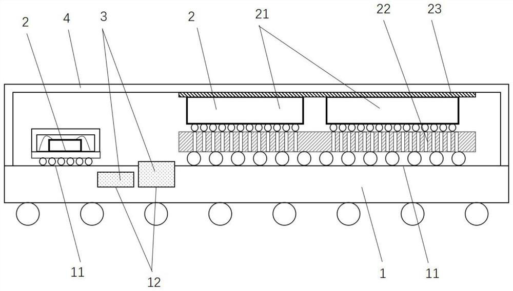
[0021] like figure 1 As shown, the three-dimensional packaging structure for multi-chip device integration in this embodiment includes a substrate 1, a chip packaging unit 2 and a working device 3. The surface of the substrate 1 is provided with a plurality of packaging areas 11 and a plurality of concave embedded In area 12, each chip packaging unit 2 is packaged and connected at the packaging area 11, and each working device 3 is embedded and connected in the embedded area 12; at least one chip packaging unit 2 includes a chip 21 and a passive silicon interposer 22, and the chip 21 is flipped and connected The top surface of the passive silicon interposer 22 is bonded and connected, and the passive silicon interposer 22 is connected to the substrate 1 through the bumps provided on the bottom surface.

[0022] In the packaging structure of this embodiment, the substrate 1 and the chip 21 are no longer correspondingly arranged, and the chip 21 and the substrate 1 are no longer...


PUM


Abstract

The invention discloses a three-dimensional packaging structure for multi-chip device integration, which comprises a substrate, chip packaging units and working devices, a plurality of packaging areas and a plurality of concave embedding areas are arranged on the surface of the substrate, each chip packaging unit is packaged and connected to the corresponding packaging area, and each working device is embedded and connected to the corresponding embedding area; and at least one chip packaging unit comprises a chip and a passive silicon interposer, the chip is inversely arranged and is in bonding connection with the top surface of the passive silicon interposer, and the passive silicon interposer is connected with the substrate through a bump arranged on the bottom surface of the passive silicon interposer. The three-dimensional packaging structure for multi-chip device integration has the advantages of being simple in arrangement, good in heat dissipation performance, not prone to warping, capable of additionally arranging packaging chips and electronic devices and the like.

Description

technical field [0001] The present invention relates to the technical field of three-dimensional packaging, in particular to a three-dimensional packaging structure for multi-chip device integration. Background technique [0002] At present, as the semiconductor process is approaching the physical limit, advanced three-dimensional packaging technology has become another way for the industry to continue Moore's Law. Advanced three-dimensional packaging enables higher system integration, smaller size, and better performance, while reducing the cost and power consumption of system integration. [0003] The existing 2.5D packaging technology mainly uses micro-bumps (u bumps) and through-silicon vias (TSV) and other technologies, and uses an interposer between the substrate and the chip to redesign the interconnection circuit, so as to achieve the chip's Stacked packages. In the packaging process, firstly, a chip to be packaged is prepared, the front of the chip has bumps, the ...

Claims


Application Information

Patent Timeline
IPC IPC(8): H01L23/13H01L23/367
CPCH01L23/13H01L23/3672
Inventor 朱文辉苏锦阳唐楚
Owner CENT SOUTH UNIV
Learn More