Superconducting quantum bit structure based on NbN Josephson junction and preparation method thereof
A superconducting quantum and bit technology, applied in the field of superconducting electronics, to achieve the effects of enhancing coherence, eliminating quantum-phonon coupling, and avoiding the formation of oxides
- Summary
- Abstract
- Description
- Claims
- Application Information
AI Technical Summary
Problems solved by technology
Method used
Image
Examples
Embodiment 1
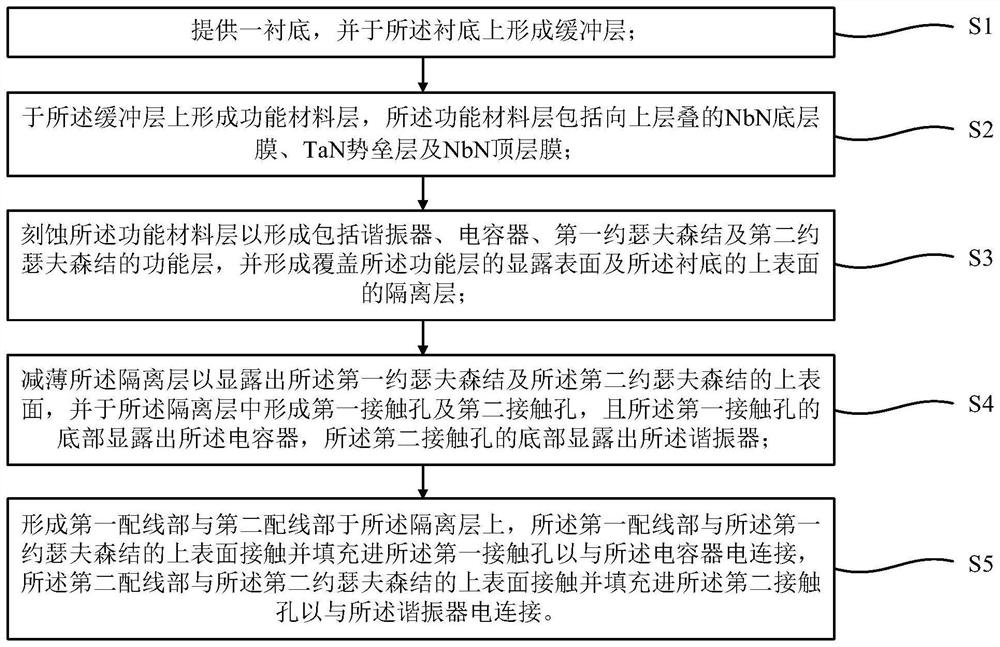
[0065] This embodiment provides a preparation method of a superconducting qubit structure based on NbN Josephson junction, such as figure 1 As shown, the flow chart of the preparation method for forming the superconducting qubit structure based on the NbN Josephson junction includes the following steps:
[0066] S1: providing a substrate, and forming a buffer layer on the substrate;
[0067] S2: forming a functional material layer on the buffer layer, the functional material layer including a NbN bottom layer, a TaN barrier layer and a NbN top layer stacked upward;
[0068] S3: Etch the functional material layer to form a functional layer including a resonator, a capacitor, a first Josephson junction and a second Josephson junction, and form an exposed surface covering the functional layer and an upper surface of the substrate the isolation layer;
[0069] S4: thinning the isolation layer to expose the upper surfaces of the first Josephson junction and the second Josephson j...
Embodiment 2
[0110] This embodiment provides a superconducting qubit structure based on NbN Josephson junction, such as Figure 10 As shown, it is a schematic cross-sectional structure diagram of the superconducting qubit structure of the NbN Josephson junction, including a substrate 1, a buffer layer 11, a functional layer 13, an isolation layer 2, a first wiring portion 31 and a second wiring portion 32, wherein the buffer layer 11 is located on the upper surface of the substrate 1, the functional layer 13 is located on the upper surface of the buffer layer 11 and includes spaced capacitors 125, a first Josephson junction 126, a second Josephson junction 127 and resonator 124, the isolation layer 2 fills the functional layer 13 between the resonator 124, the capacitor 125, the first Josephson junction 126 and the second Josephson junction 127 and cover the exposed surfaces of the resonator 124 and the capacitor 125 and the upper surface of the substrate 1, and the isolation layer 2 is pr...
PUM
| Property | Measurement | Unit |
|---|---|---|
| Thickness | aaaaa | aaaaa |
| Thickness | aaaaa | aaaaa |
| Thickness | aaaaa | aaaaa |
Abstract
Description
Claims
Application Information
 - R&D
- Intellectual Property
- Life Sciences
- Materials
- Tech Scout
- Unparalleled Data Quality
- Higher Quality Content
- 60% Fewer Hallucinations
Browse by: Latest US Patents, China's latest patents, Technical Efficacy Thesaurus, Application Domain, Technology Topic, Popular Technical Reports.
© 2025 PatSnap. All rights reserved.Legal|Privacy policy|Modern Slavery Act Transparency Statement|Sitemap|About US| Contact US: help@patsnap.com


