Three-dimensional fan-out packaging structure and preparation method thereof
A packaging structure, three-dimensional technology, applied in semiconductor/solid-state device manufacturing, semiconductor/solid-state device components, semiconductor devices, etc., can solve problems such as affecting service life, long interconnection distance, unstable performance of semiconductor core particles, etc. The effect of large bump area, high component reliability and flexible contact pitch
Inactive Publication Date: 2022-05-31
WUHAN UNIV
View PDF6 Cites 2 Cited by
- Summary
- Abstract
- Description
- Claims
- Application Information
AI Technical Summary
Problems solved by technology
[0003] At present, for semiconductor stacking components, it is usually to stack multiple semiconductor chips together through bonding materials, and then use molding materials or underfill materials to package the stacked semiconductor chips to form a semiconductor stacked package structure, and in the actual application process , when different types of semiconductor chips are stacked together, due to their long interconnection distance, the performance of semiconductor chips will be unstable, which will affect their service life
Method used
View moreImage
Smart ImageViewing Examples


Examples
Embodiment 1
Embodiment 2
Embodiment 3
Login to View More PUM
 Abstract
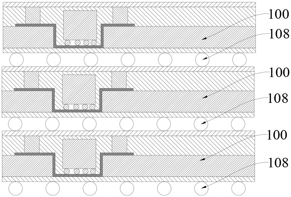
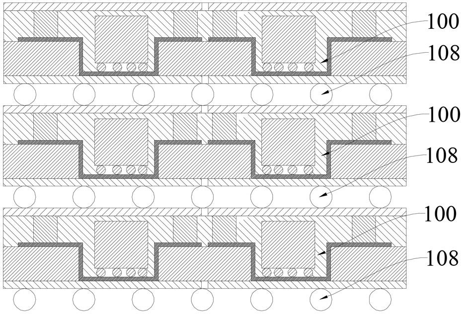
The invention discloses a three-dimensional fan-out packaging structure and a preparation method thereof, and the method comprises the steps: digging a groove in a carrier plate, preparing a metal wiring layer at the groove and the periphery of the groove, then pasting a core particle, leading out a part of pins of the core particle to the front surface of the carrier plate through the metal wiring layer, carrying out the plastic packaging, preparing a conductive column at a plastic packaging layer, and leading out the part of pins. Then preparing a first rewiring layer and a first dielectric layer on the plastic packaging layer to complete front packaging; and thinning the back surface of the carrier plate until the metal wiring layer is formed and the other part of pins of the core particles are exposed, then preparing a second rewiring layer and a second dielectric layer, completing preparation of fan-out packaging units of double-sided fan-out, stacking the fan-out packaging units according to needs, and then connecting the fan-out packaging units by adopting solder balls to obtain the three-dimensional fan-out packaging structure. According to the fan-out packaging unit with the two fan-out surfaces, the interconnection distance can be effectively reduced, three-dimensional stacking is facilitated, the fan-out packaging unit has great advantages in electrical interconnection performance, the loss is smaller, the efficiency is higher, the packaging process difficulty is greatly reduced, and the packaging cost is reduced.
Description
A three-dimensional fan-out packaging structure and preparation method thereof technical field The invention belongs to the technical field of integrated circuit packaging, relate to a kind of fan-out packaging technology, be specifically related to a kind of three-dimensional Fan-out package structure and preparation method thereof. Background technique [0002] With the improvement of IC technology, the chip area is constantly shrinking, and the number of transistors contained in a unit area is increasing. Plus, the chip cannot accommodate enough pins per unit area, and the traditional package cannot meet the high-resolution chip package. Therefore, the high-density fan-out packaging method came into being. Wafer-level fan-out packaging is an embedded package fabricated at the wafer level. It is also a major advanced technology for the large number of input / output ports (I / O) and high integration flexibility. packaging process. It can realize vertical and horizon...
Claims
Login to View More Application Information
Patent Timeline
 Patent Type & Authority Applications(China)
IPC IPC(8): H01L23/498H01L21/48H01L21/52H01L23/49H01L21/60
CPCH01L23/49838H01L23/49816H01L23/49H01L21/4853H01L21/52H01L24/81H01L2224/02379H01L2224/02381H01L2224/0231H01L2224/02331H01L2924/181H01L2224/16225H01L2924/00012
Inventor 刘胜王诗兆张贺辉刘天建田志强周振东芳
Owner WUHAN UNIV
Features
- R&D
- Intellectual Property
- Life Sciences
- Materials
- Tech Scout
- Unparalleled Data Quality
- Higher Quality Content
- 60% Fewer Hallucinations
Learn More Browse by: Latest US Patents, China's latest patents, Technical Efficacy Thesaurus, Application Domain, Technology Topic, Popular Technical Reports.
© 2025 PatSnap. All rights reserved.Legal|Privacy policy|Modern Slavery Act Transparency Statement|Sitemap|About US| Contact US: help@patsnap.com