Long-wavelength led homoepitaxial structure, its preparation method and application
A homoepitaxial, long-wavelength technology, applied in semiconductor devices, electrical components, circuits, etc., can solve the problems of reduced atomic migration ability, difficulty in epitaxial growth, and increased defect surface, so as to improve incorporation efficiency, promote popularization and application, The effect of improving quantum efficiency
- Summary
- Abstract
- Description
- Claims
- Application Information
AI Technical Summary
Problems solved by technology
Method used
Image

Examples
preparation example Construction
[0076] In one embodiment, the preparation method specifically includes:
[0077] at a first temperature, sequentially forming a porous structure layer, a first InGaN layer and a first GaN layer on the substrate, thereby forming the buffer layer;
[0078] growing a relaxation layer on the buffer layer at a second temperature, the first temperature < the second temperature;
[0079] growing a stress release layer on the relaxation layer at a third temperature, where the first temperature
[0080] A multi-quantum well light-emitting layer is grown on the stress release layer at a fourth temperature, where the first temperature≤fourth temperature≤third temperature.
[0081] In one embodiment, the preparation method specifically includes:
[0082] First, at a fifth temperature, a polycrystalline material layer or an amorphous material layer is grown on the substrate, and then at a first temperature, a first InGaN layer is sequenti...
Embodiment 1
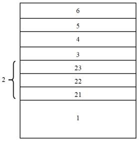
[0102] A long-wavelength LED homoepitaxial structure can refer to figure 1 , its preparation method comprises the steps:
[0103] (1) Put the n-type GaN single crystal substrate into the growth chamber of the MOCVD equipment, set the temperature in the growth chamber to about 750 °C, and first grow a porous SiN layer with a thickness of about 5 nm on the substrate. Temperature about 800℃, SiH 4 The throughput is about 5slm, NH 3 The flow rate is about 50slm, the growth time is about 60s-120s, the pore size of the pores contained in the formed porous structure is about 10nm-100nm, and the porosity is about 10%-30%, and then continue to grow on the porous SiN layer. a first InGaN layer with a thickness of about 5 nm, a first GaN layer with a thickness of about 5 nm, thereby forming a buffer layer;
[0104] (2) Raising the temperature in the growth chamber to about 850° C., and growing a first InGaN / GaN superlattice on the buffer layer, the thickness of a single GaN layer in t...
Embodiment 2
[0145] A long-wavelength LED homoepitaxial structure can also refer to figure 1 , its preparation method comprises the steps:
[0146] (1) Put the n-type GaN single crystal substrate into the growth chamber of the MOCVD equipment, set the temperature in the growth chamber to about 700 °C, and first grow a porous SiN layer with a thickness of about 1 nm on the substrate. Temperature about 850℃, SiH 4 The throughput is about 2slm, NH 3 The input amount is about 20slm, the growth time is about 60s-80s, and then the first InGaN layer with a thickness of about 10nm and a first GaN layer with a thickness of about 10nm are continuously grown on the porous SiN layer to form a buffer layer;
[0147] (2) Raising the temperature in the growth chamber to about 900° C., and growing a first InGaN / GaN superlattice on the buffer layer, the thickness of a single GaN layer in the first InGaN / GaN superlattice About 2nm, the thickness of a single InGaN layer is about 10 times that of a single ...
PUM
| Property | Measurement | Unit |
|---|---|---|
| pore size | aaaaa | aaaaa |
| thickness | aaaaa | aaaaa |
| thickness | aaaaa | aaaaa |
Abstract
Description
Claims
Application Information
 - Generate Ideas
- Intellectual Property
- Life Sciences
- Materials
- Tech Scout
- Unparalleled Data Quality
- Higher Quality Content
- 60% Fewer Hallucinations
Browse by: Latest US Patents, China's latest patents, Technical Efficacy Thesaurus, Application Domain, Technology Topic, Popular Technical Reports.
© 2025 PatSnap. All rights reserved.Legal|Privacy policy|Modern Slavery Act Transparency Statement|Sitemap|About US| Contact US: help@patsnap.com