Multifunctional photosensitive synaptic device based on two-dimensional material and preparation method of multifunctional photosensitive synaptic device

A technology of two-dimensional materials and synaptic devices, which is applied in semiconductor devices, electrical components, biological neural network models, etc., can solve problems such as difficulty in improving integration and establishment of artificial neural networks, and achieve simple and easy-to-understand working principles and structural Simple, highly photoresponsive effects

Pending Publication Date: 2022-05-13
ZHEJIANG UNIV HANGZHOU GLOBAL SCI & TECH INNOVATION CENT
View PDF0 Cites 0 Cited by
  • Summary
  • Abstract
  • Description
  • Claims
  • Application Information

AI Technical Summary

Problems solved by technology

[0004] Artificial synaptic devices based on traditional CMOS require multiple transistors to simulate a synaptic behavior, making it difficult to increase the integration level, which brings difficulties and challenges to the establishment of high-density artificial neural networks

Method used


Image

  • Multifunctional photosensitive synaptic device based on two-dimensional material and preparation method of multifunctional photosensitive synaptic device
  • Multifunctional photosensitive synaptic device based on two-dimensional material and preparation method of multifunctional photosensitive synaptic device
  • Multifunctional photosensitive synaptic device based on two-dimensional material and preparation method of multifunctional photosensitive synaptic device

Examples


Embodiment 1

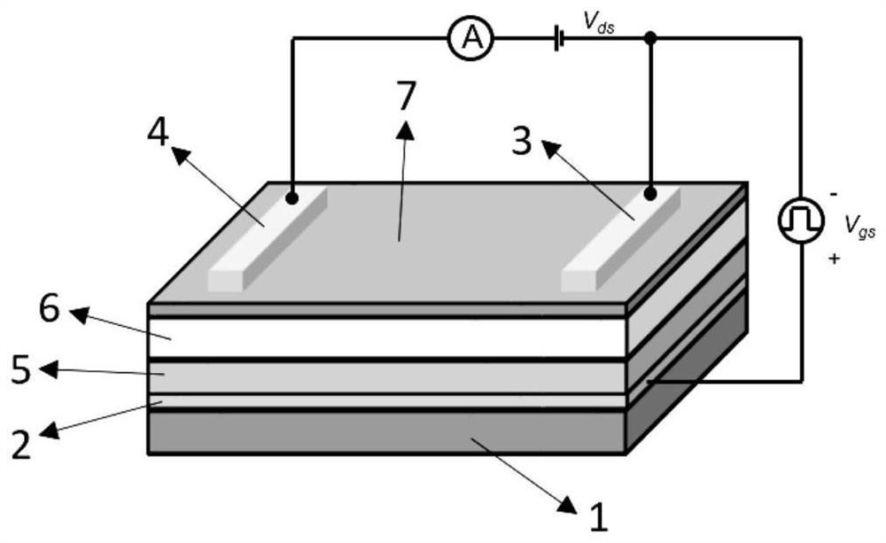
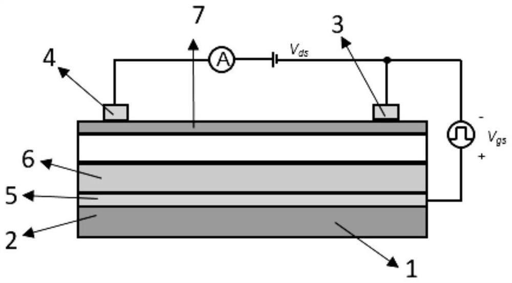
[0049] A multifunctional photosensitive synaptic device based on two-dimensional materials such as Figure 1-2 shown, including:

[0050] substrate1;

[0051] The gate 2, the source 3, the drain 4 and the stacked structure arranged above the oxide layer of the substrate 1, the stacked structure includes a first two-dimensional material layer 5, a second two-dimensional material layer 6 and a third two-dimensional material layer layer 7, the gate 2 is arranged above the substrate 1, and the gate 2 covers the first two-dimensional material layer 5, the second two-dimensional material layer 6 and the third two-dimensional material layer 7 in sequence, and the third two-dimensional material layer The top of the two-dimensional material layer 7 covers the source electrode 3 and the drain electrode 4 respectively, and a channel is formed between the source electrode 3 and the drain electrode 4, wherein the second two-dimensional material layer 6 includes hexagonal boron nitride in ...

Embodiment 2

[0059] The following is an example procedure:

[0060] A method for preparing a multifunctional photosensitive synaptic device based on two-dimensional materials, comprising the following steps:

[0061] S100, providing a substrate 1, the substrate 1 is an insulating material substrate or the top layer of the substrate 1 is an insulating material layer;

[0062] S200, forming a gate 2 on the oxide layer of the substrate 1;

[0063] S300, the top of the gate 2 is sequentially covered with a stack structure, the stack structure includes a first two-dimensional material layer 5, a second two-dimensional material layer 6, and a third two-dimensional material layer 7, wherein the second two-dimensional material layer 6 contains hexagonal boron nitride in a defect state, the first two-dimensional material layer 5 is used as a light absorbing layer, the second two-dimensional material layer 6 is used as an intermediate isolation layer, and the third two-dimensional material layer 7 ...

Embodiment 3

[0083] A multifunctional photosensitive synaptic device based on two-dimensional materials such as Figure 6-7 shown, including:

[0084] A substrate 1, the substrate 1 is an insulating material substrate or the top layer of the substrate is an insulating material layer;

[0085] The gate 2, the source 3, the drain 4 and the stacked structure arranged above the oxide layer of the substrate 1, the stacked structure includes a first two-dimensional material layer 5, a second two-dimensional material layer 6 and a third two-dimensional material layer Layer 7, the gate 2 is arranged above the substrate 1, and the gate 2 covers the first two-dimensional material layer 5, the second two-dimensional material layer 6 and the third two-dimensional material layer 7 in sequence, and includes two gates pole 2 and two first two-dimensional material layers 5, a first channel 8 is formed between the two gates 2, the two first two-dimensional material layers 5 are respectively arranged above...


PUM


Abstract

The invention discloses a multifunctional photosensitive synapse device based on a two-dimensional material and a preparation method thereof, the device comprises a substrate, a grid electrode, a source electrode, a drain electrode and a stacking structure, the grid electrode, the source electrode, the drain electrode and the stacking structure are arranged on the substrate, the stacking structure comprises a first two-dimensional material layer, a second two-dimensional material layer and a third two-dimensional material layer, the grid electrode is arranged on the substrate, and the third two-dimensional material layer is arranged on the substrate. A first two-dimensional material layer, a second two-dimensional material layer and a third two-dimensional material layer are sequentially covered on the grid electrode, a source electrode and a drain electrode are respectively covered on the third two-dimensional material layer, and a channel is formed between the source electrode and the drain electrode. The second two-dimensional material layer comprises hexagonal boron nitride in a defect state, the first two-dimensional material layer serves as a light absorption layer, the second two-dimensional material layer serves as an isolation layer, and the third two-dimensional material layer serves as a readout layer. The device is simple in structure, simple and understandable in working principle, simple in preparation process and easy to master; based on vertical stacking of pure two-dimensional thin film materials, the size is small, and the requirements for high density and high integration level are met.

Description

technical field [0001] The invention relates to the technical field of semiconductor devices, in particular to a multifunctional photosensitive synapse device based on two-dimensional materials and a preparation method thereof. Background technique [0002] With the further development of artificial intelligence, efficient data access and massive data storage requirements have posed increasing challenges to the traditional von Neumann architecture system in which computing modules and storage units are independent. At the same time, the development of semiconductor technology has been Approaching the limit of Moore's Law, it is becoming more and more difficult to improve the performance of the von Neumann architecture by improving the process. Neuromorphic computing, which processes data by simulating neurons and synapses in the biological brain, has become an important direction for the development of high-performance computing due to its advantages of low energy consumptio...

Claims


Application Information

Patent Timeline
Patent Type & Authority Applications(China)
IPC IPC(8): H01L31/0328H01L31/0392H01L31/112H01L31/18G06N3/06
CPCH01L31/0328H01L31/0392H01L31/112H01L31/18G06N3/061
Inventor 徐杨周嘉超李涵茜徐心艺田丰陈丽陈安哲俞滨
Owner ZHEJIANG UNIV HANGZHOU GLOBAL SCI & TECH INNOVATION CENT
Why Eureka
Try Eureka