Integrated self-biased pMOS low turn-off loss SJ-LIGBT device
A technology of turn-off loss and self-biasing, applied in the field of SJ-LIGBT devices, can solve the problems of device influence, no carrier extraction channel, tail current with long turn-off time, etc., to reduce the saturation current density and optimize the electric field. , Enhance the effect of short-circuit safe working characteristics
- Summary
- Abstract
- Description
- Claims
- Application Information
AI Technical Summary
Problems solved by technology
Method used
Image

Examples
Embodiment 1
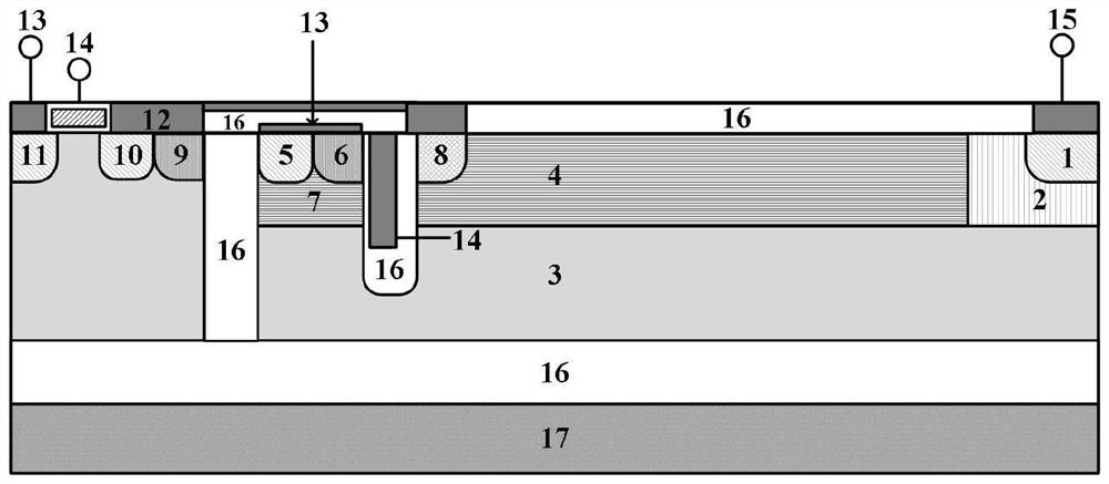
[0041] figure 1 It is an SJ-LIGBT device with integrated self-biased pMOS and low turn-off loss proposed by the present invention, and it is a schematic structural diagram of Embodiment 1. Self-biased pMOS includes P+ drain, N-type region, P+ source, metal gate and trench gate short circuit, no additional gate signal control is required. The pMOS source is shorted to the LIGBT drift region.
[0042] Such as figure 1 As shown, the implementation of the present invention proposes an integrated self-biased pMOS low turn-off loss SJ-LIGBT device, the LIGBT device includes a P+ collector 1, an N-type buffer layer 2, an N-type drift region 3, and a P-column region 4. P+ emitter 5, N+ electron emitter 6, P-body7, P-top region 8, N-type region 9, P+ source 10, P+ drain 11, floating ohmic contact 12, emitter 13, gate 14. A collector electrode 15, a silicon dioxide insulating layer 16, and a P-type substrate 17. The SJ-LIGBT device integrating self-biased pMOS low turn-off loss is c...
Embodiment 2
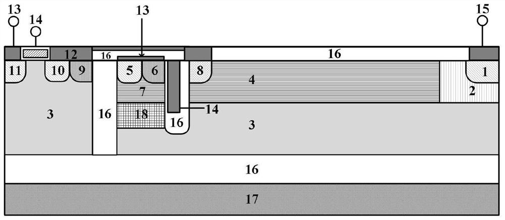
[0046] figure 2 A schematic structural diagram of Embodiment 2 of the LIGBT device provided by the present invention. On the basis of Example 1, an N-type hole blocking layer is introduced on the lower side of the p-body, the lower side of the p-body is flush with the upper side of the N-type hole blocking layer, and the lower side is flush with the upper side of the N-type drift region. Side flush.
[0047] Such as figure 2As shown, the implementation of the present invention proposes an integrated self-biased pMOS low turn-off loss SJ-LIGBT device, the LIGBT device includes a P+ collector 1, an N-type buffer layer 2, an N-type drift region 3, and a P-column region 4. P+ emitter 5, N+ electron emitter 6, P-body7, P-top region 8, N-type region 9, P+ source 10, P+ drain 11, floating ohmic contact 12, emitter 13, gate 14. A collector electrode 15, a silicon dioxide insulating layer 16, a P-type substrate 17, and a hole blocking layer 18. The SJ-LIGBT device integrating sel...
Embodiment 3
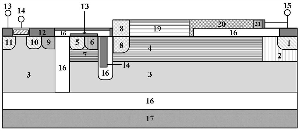
[0051] Such as figure 1 As shown, the implementation of the present invention proposes an integrated self-biased pMOS low turn-off loss SJ-LIGBT device, the LIGBT device includes a P+ collector 1, an N-type buffer layer 2, an N-type drift region 3, and a P-column region 4. P+ emitter 5, N+ electron emitter 6, P-body7, P-top region 8, N-type region 9, P+ source 10, P+ drain 11, floating ohmic contact 12, emitter 13, gate 14. Collector electrode 15, silicon dioxide insulating layer 16, P-type substrate 17, P-surface layer 19, N-isolating region 20, N+ surface layer 21. The SJ-LIGBT device integrating self-biased pMOS low turn-off loss is characterized in that 1. The device is divided into a pMOS region, a PN junction region and a LIGBT region from left to right, and the LIGBT region includes a P+ collector 1. N-type buffer layer 2, N-type drift region 3, P column region 4, P+ emitter 5, N+ electron emitter 6, P-body7, P-top region 8, emitter 13, gate 14, collector 15. A silico...
PUM
| Property | Measurement | Unit |
|---|---|---|
| length | aaaaa | aaaaa |
| thickness | aaaaa | aaaaa |
| length | aaaaa | aaaaa |
Abstract
Description
Claims
Application Information
 - Generate Ideas
- Intellectual Property
- Life Sciences
- Materials
- Tech Scout
- Unparalleled Data Quality
- Higher Quality Content
- 60% Fewer Hallucinations
Browse by: Latest US Patents, China's latest patents, Technical Efficacy Thesaurus, Application Domain, Technology Topic, Popular Technical Reports.
© 2025 PatSnap. All rights reserved.Legal|Privacy policy|Modern Slavery Act Transparency Statement|Sitemap|About US| Contact US: help@patsnap.com