Display panel and display terminal
A display panel and terminal technology, applied in semiconductor devices, electrical components, circuits, etc., can solve the problems of small drilling process window, poor electrical connection between display components and drive substrates, and decline in display panel yield
- Summary
- Abstract
- Description
- Claims
- Application Information
AI Technical Summary
Problems solved by technology
Method used
Image
Examples
Embodiment 1
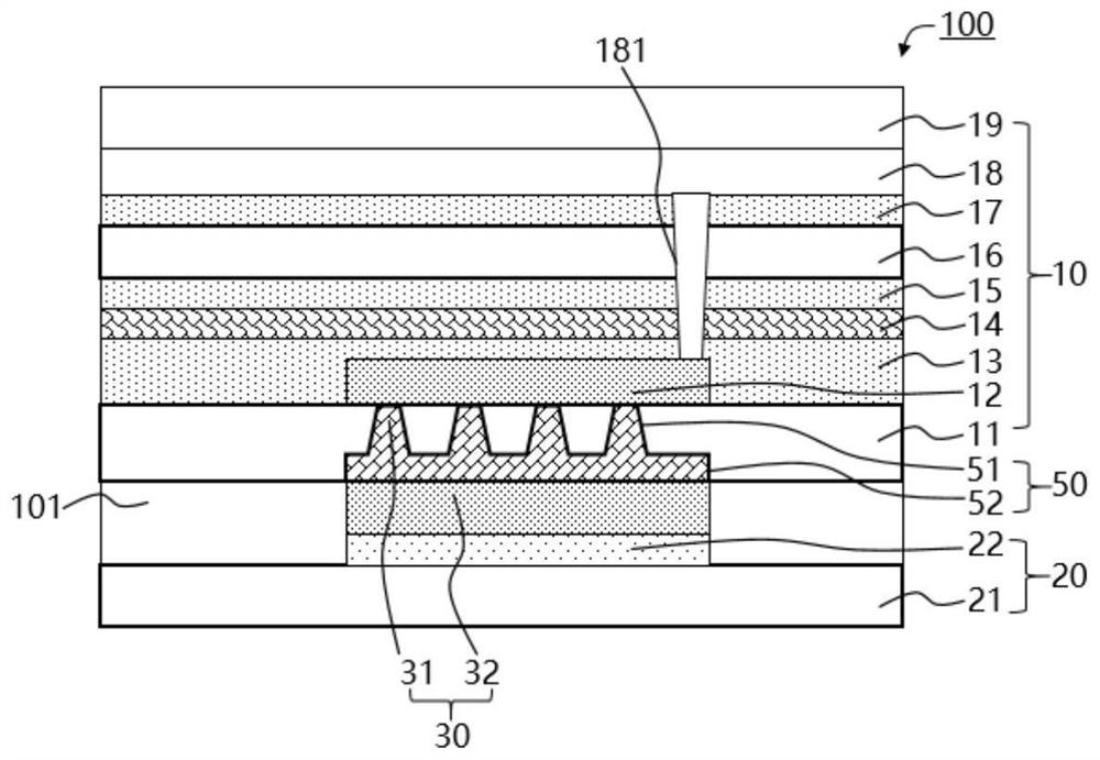
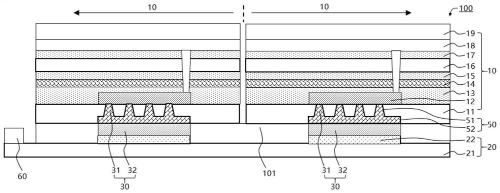
[0050] see figure 1 , figure 2 , Figure 3(a), Figure 3(b), Figure 3(c), figure 1 The first schematic diagram of the display panel 100 provided by the embodiment of the present application; figure 2 A schematic diagram of a splicing state of the display panel 100 provided by the embodiment of the present application; FIG. 3( c ) is a schematic cross-sectional view of the sub-through hole 51 provided by the embodiment of the present application when there is a groove 52 .
[0051] The embodiment of the present application provides a display panel 100. The display panel 100 includes: at least one display component 10, a driving substrate 20, and a conductive member 30. The display component 10 includes a first base 11, and at least A first terminal 12, and a light-emitting layer 19, the light-emitting layer 19 is electrically connected to the first terminal 12; the driving substrate 20 includes a driving chip 60, a second base 21, and a plurality of second terminals 22 arran...
Embodiment 2
[0092] This embodiment is the same or similar to the display panel in the above embodiments, except that the sub-through hole 51 also extends to the inside of the first terminal 12 .
[0093] see Figure 4 , Figure 4 It is a second schematic diagram of the display panel 100 provided by the embodiment of the present application.
[0094] The embodiment of the present application provides a display panel 100 . Compared with the first embodiment, the sub-through hole 51 also extends to the inside of the first terminal 12 .
[0095] Specifically, when a plurality of sub-vias 51 are formed by laser, the sub-vias 51 also extend to the inside of the first terminal 12 at the same time.
[0096] Specifically, when the first sub-vias 31 are formed in the sub-vias 51 , the first sub-vias 31 also fill the part of the sub-vias 51 extending to the inside of the first terminal 12 .
[0097] In the embodiment of the present application, the arrangement of the through hole group 50 also ha...
Embodiment 3
[0101] This embodiment is the same as or similar to the display panel in the above embodiments, except that the sub-through hole 51 also passes through the first terminal 12 .
[0102] see Figure 5 , Figure 5 It is a third schematic diagram of the display panel 100 provided by the embodiment of the present application.
[0103] In the embodiment of the present application, compared with the first and second embodiments, the sub-through hole 51 also penetrates the first terminal 12 .
[0104] Specifically, in some implementation situations, the size of the first terminal 12 is small and the thickness is relatively thin, and when the sub-through hole 51 does not penetrate the first terminal 12, the contact area between the first terminal 12 and the side surface of the conducting member 30 is not large enough. .
[0105] Specifically, when the sub-through hole 51 also passes through the first terminal 12 , the contact area of the first terminal 12 with the side surface of ...
PUM
| Property | Measurement | Unit |
|---|---|---|
| Length | aaaaa | aaaaa |
Abstract
Description
Claims
Application Information
 - R&D Engineer
- R&D Manager
- IP Professional
- Industry Leading Data Capabilities
- Powerful AI technology
- Patent DNA Extraction
Browse by: Latest US Patents, China's latest patents, Technical Efficacy Thesaurus, Application Domain, Technology Topic, Popular Technical Reports.
© 2024 PatSnap. All rights reserved.Legal|Privacy policy|Modern Slavery Act Transparency Statement|Sitemap|About US| Contact US: help@patsnap.com


