


Quick Research
Generate reliable direction feasibility study reports for your R&D in just a few steps.

Technical Q&A
Discover and master advanced knowledge NOW. Basics, ideas, possibilities, all at once.

Find Solutions
As an expert in R&D theories, this can generate solutions to your technical problems instantly.

Evaluate Feasibility
Analyze your overall solution with one click, know your potential R&D risks in advance.

Monitor Landscape
Get weekly tech updates, stay abreast of the latest tech innovations and key insights.
Perovskite thin film manufacturing method, solar cell and laminated cell
A production method and technology of perovskite, applied in circuits, photovoltaic power generation, electrical components, etc., can solve problems such as difficulty in organic components, short circuit of batteries, reaction of inorganic components, etc.
- Summary
- Abstract
- Description
- Claims
- Application Information
AI Technical Summary
Problems solved by technology
Method used
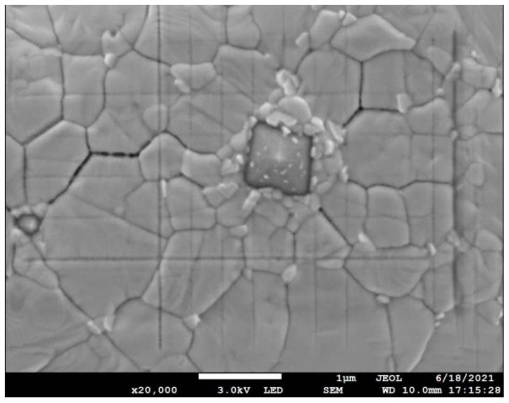
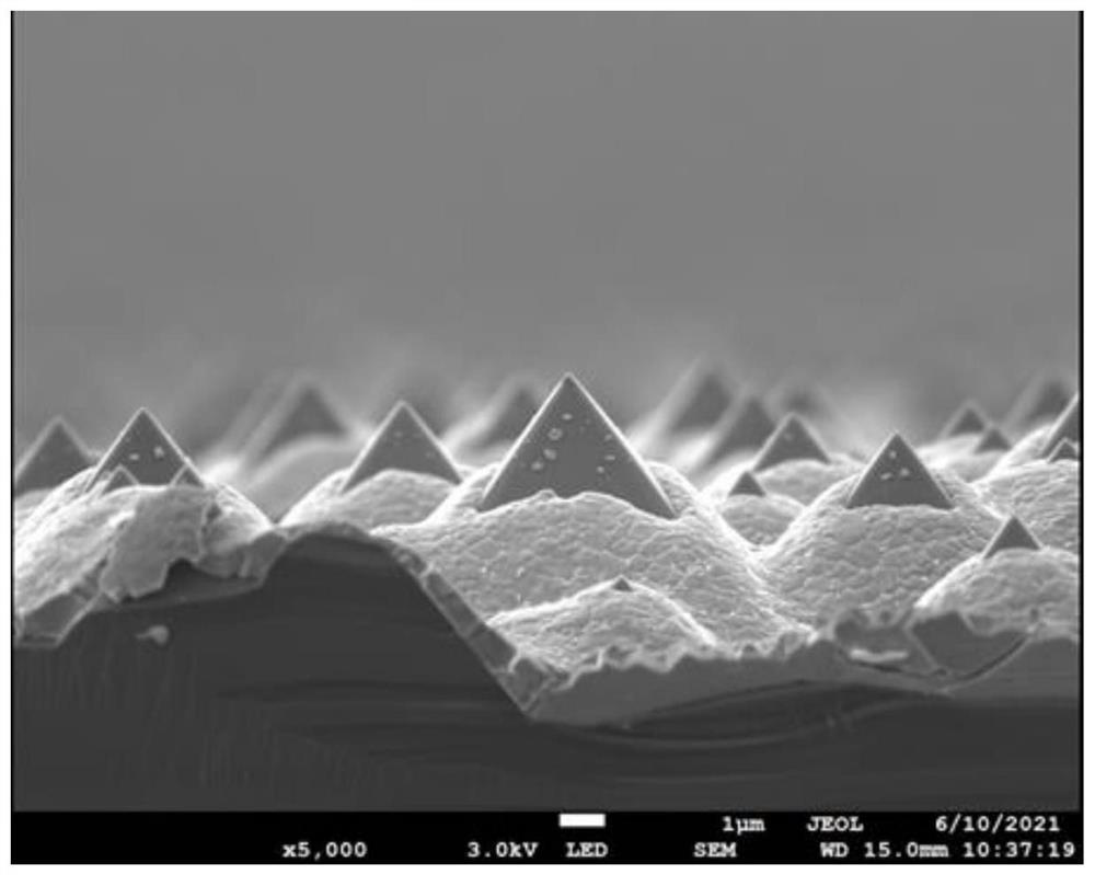
Image

Examples
Embodiment 1
[0085] The application of the manufacturing method of the perovskite thin film provided in the embodiment of the present invention in the laminated battery is as follows:
[0086] The first step is to provide a commercial-grade M2 n-type silicon wafer with a thickness of 180um and a resistivity of 5Ω·cm, which is polished with an alkaline solution, textured, and cleaned to form an n-type silicon wafer substrate with a pyramid textured surface.
[0087] In the second step, in a plasma-enhanced chemical vapor deposition (PECVD) device, a 10nm intrinsic amorphous silicon passivation layer is sequentially deposited on the front and back of the n-type silicon wafer substrate to passivate the dangling bonds on the surface of the crystalline silicon.
[0088] In the third step, the n-type amorphous silicon emission level is deposited with a thickness of 10nm by using the mixed gas of phosphine and silane diluted with hydrogen, and the p-type amorphous silicon back layer with a thick...
Embodiment 2
[0099] The application of the manufacturing method of the perovskite thin film provided in the embodiment of the present invention in the laminated battery is as follows:
[0100] The first step is to provide a commercial-grade M2 n-type silicon wafer with a thickness of 180um and a resistivity of 5Ω·cm, which is polished with an alkaline solution, textured, and cleaned to form an n-type silicon wafer substrate with a pyramid textured surface.
[0101] In the second step, in a plasma-enhanced chemical vapor deposition (PECVD) device, a 10nm intrinsic amorphous silicon passivation layer is sequentially deposited on the front and back of the n-type silicon wafer substrate to passivate the dangling bonds on the surface of the crystalline silicon.
[0102] In the third step, the n-type amorphous silicon emission level is deposited with a thickness of 10nm by using the mixed gas of phosphine and silane diluted with hydrogen, and the p-type amorphous silicon back layer with a thick...
Embodiment 3
[0112] The application of the manufacturing method of the perovskite thin film provided in the embodiment of the present invention in the laminated battery is as follows:
[0113] The first step is to provide a commercial-grade M2 n-type silicon wafer with a thickness of 180um and a resistivity of 5Ω·cm, which is polished with an alkaline solution, textured, and cleaned to form an n-type silicon wafer substrate with a pyramid textured surface.
[0114] In the second step, in a plasma-enhanced chemical vapor deposition (PECVD) device, a 10nm intrinsic amorphous silicon passivation layer is sequentially deposited on the front and back of the n-type silicon wafer substrate to passivate the dangling bonds on the surface of the crystalline silicon.
[0115] In the third step, the n-type amorphous silicon emission level is deposited with a thickness of 10nm by using the mixed gas of phosphine and silane diluted with hydrogen, and the p-type amorphous silicon back layer with a thick...
PUM
| Property | Measurement | Unit |
|---|---|---|
| Thickness | aaaaa | aaaaa |
| Thickness | aaaaa | aaaaa |
| Resistivity | aaaaa | aaaaa |
Abstract
Description
Claims
Application Information
 - R&D Engineer
- R&D Manager
- IP Professional
- Industry Leading Data Capabilities
- Powerful AI technology
- Patent DNA Extraction
Browse by: Latest US Patents, China's latest patents, Technical Efficacy Thesaurus, Application Domain, Technology Topic, Popular Technical Reports.
© 2024 PatSnap. All rights reserved.Legal|Privacy policy|Modern Slavery Act Transparency Statement|Sitemap|About US| Contact US: help@patsnap.com