Array substrate, display panel and display device
An array substrate and display panel technology, applied in nonlinear optics, instruments, optics, etc., can solve the problem of inconvenient detection of abnormal signals of the array substrate, and achieve the effect of convenient signal detection
- Summary
- Abstract
- Description
- Claims
- Application Information
AI Technical Summary
Problems solved by technology
Method used
Image
Examples
no. 1 example
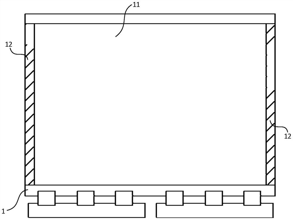
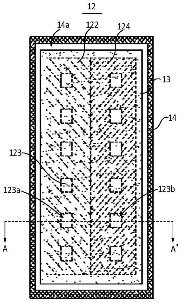
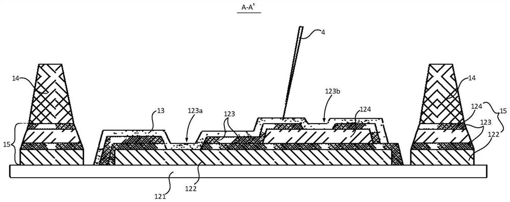
[0051] combine Figures 1 to 3 As shown, the present application proposes an array substrate 1. The array substrate 1 has a display area 11 and a non-display area 12 surrounding the display area 11. A test electrode 13 is provided in the non-display area 12. The test electrode 13 is used for Input a test signal into the display area 11, the array substrate 1 includes a spacer 14, the spacer 14 is arranged in the non-display area 12, and is at least partly located above the test electrode 13, and the spacer 14 is provided with probes for detection 4 through the escape channel 14a, the avoidance channel 14a runs through the spacer 14 and extends to the test electrode 13.
[0052] In this example, if figure 1 As shown, the display area 11 of the array substrate 1 is located in the middle of the array substrate 1 , and the non-display area 12 of the array substrate 1 is arranged around the display area 11 of the array substrate 1 . The display area 11 of the array substrate 1 ca...
no. 2 example
[0072] The present application also proposes a display panel, such as Figure 10 As shown, the display panel includes the above-mentioned array substrate 1 and color filter substrate 2. The color filter substrate 2 is disposed on one side of the array substrate 1 and surrounds the array substrate 1 to form a sealed space that can be filled with liquid crystals.
[0073] In this embodiment, the color filter substrate 2 is disposed on the opposite side of the array substrate 1, and surrounds the array substrate 1 to form a liquid crystal cell, and the sealed space in the liquid crystal cell is used for filling liquid crystals. The test electrode 13 and the spacer 14 are located between the color filter substrate 2 and the array substrate 1, the test electrode 13 is located in the non-display area 12 of the array substrate 1, and the non-display area of the color filter substrate 2 corresponds to the non-display area of the array substrate 1 12, the non-display area of the ...
no. 3 example
[0075] The present application also proposes a display device, such as Figure 11 As shown, the display device includes a backlight module 3 and the display panel in the previous embodiment. The backlight module 3 is located on the side of the array substrate 1 of the display panel facing away from the color filter substrate 2 of the display panel, and is used to provide Provide a light source.
[0076] In this embodiment, the backlight module 3 can be a direct-type backlight module 3 or an edge-type backlight module 3, and the backlight module 3 can include a light-adjusting film such as a diffusion sheet, a backplane, a light source, a light guide plate, and other structures. The light emitting side of the backlight module 3 is set towards the array substrate 1 of the display panel, so that the backlight module 3 can provide light source to the display panel, so that the display panel can control the transmission of light and finally display images. Wherein, the specific st...
PUM
 Abstract
Description
Claims
Application Information
 - R&D Engineer
- R&D Manager
- IP Professional
- Industry Leading Data Capabilities
- Powerful AI technology
- Patent DNA Extraction
Browse by: Latest US Patents, China's latest patents, Technical Efficacy Thesaurus, Application Domain, Technology Topic, Popular Technical Reports.
© 2024 PatSnap. All rights reserved.Legal|Privacy policy|Modern Slavery Act Transparency Statement|Sitemap|About US| Contact US: help@patsnap.com


