
Growth method of superlattice detector material and superlattice infrared detector

A growth method and superlattice technology, which are applied in the growth of polycrystalline materials, crystal growth, single crystal growth, etc., can solve the problems affecting the interface quality at the connection of the functional layer of the superlattice detector, the increase of the As pressure in the cavity, and the growth beam. flow disturbance and other problems, to achieve the effect of reducing the growth beam disturbance, improving the utilization rate, and improving the uniformity of the composition

Active Publication Date: 2022-04-05
WUHAN GAOXIN TECH
View PDF4 Cites 0 Cited by
  • Summary
  • Abstract
  • Description
  • Claims
  • Application Information

AI Technical Summary

Problems solved by technology

During the growth process of existing superlattice detector materials, when growing the barrier layer, it is necessary to raise the temperature of the source furnace for the source material required for the growth of the barrier layer to the growth temperature in advance and wait for a long time. On the one hand, it will cause waste of raw materials; This will lead to the increase of As pressure in the cavity, the fluctuation of the temperature field in the cavity, and the disturbance of the growth beam, which will affect the quality of the interface at the junction of the functional layers of the superlattice detector.

Method used


Image

  • Growth method of superlattice detector material and superlattice infrared detector
  • Growth method of superlattice detector material and superlattice infrared detector

Examples


Embodiment Construction

[0026] The following will clearly and completely describe the technical solutions in the embodiments of the present invention with reference to the accompanying drawings in the embodiments of the present invention. Obviously, the described embodiments are only some, not all, embodiments of the present invention. Based on the embodiments of the present invention, all other embodiments obtained by persons of ordinary skill in the art without making creative efforts belong to the protection scope of the present invention.

[0027] In describing the present invention, it is to be understood that the terms "center", "upper", "lower", "front", "rear", "left", "right", "vertical", "horizontal", The orientations or positional relationships indicated by "top", "bottom", "inner", "outer", etc. are based on the orientations or positional relationships shown in the drawings, and are only for the convenience of describing the present invention and simplifying the description, rather than in...


PUM

PropertyMeasurementUnit
surface roughnessaaaaaaaaaa

Abstract

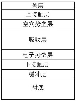
The invention provides a growth method of a superlattice detector material, which comprises the following steps of: preparing a substrate, and performing high-temperature deoxidation treatment on the substrate in a vacuum growth chamber; the method comprises the following steps: sequentially growing a plurality of superlattice detector functional layers on a substrate from bottom to top, pausing the growth between any two adjacent superlattice detector functional layers after the previous superlattice detector functional layer is grown, and infiltrating and processing the superlattice surface by using a V-group element, and meanwhile, after the temperature of the source furnace of the source material required by the growth of the next superlattice detector functional layer is increased to the growth temperature and reaches a stable state, the growth of the next superlattice detector functional layer is completed. A growth pause is inserted between the growth of two different superlattice detector functional layers, and V-group elements are used for protection in the growth pause process, so that background As voltage fluctuation can be effectively reduced, mutual mixing of As and Sb elements between the superlattice detector functional layers is reduced, and the interface quality at the joint of the superlattice detector functional layers is improved.

Description

technical field [0001] The invention belongs to the technical field of semiconductor materials and devices, and in particular relates to a growth method of a superlattice detector material and a superlattice infrared detector. Background technique [0002] The antimonide-based class II superlattice detector material based on III-V semiconductors is a new type of infrared detector material, which has the characteristics of wide-band precise adjustment, high quantum efficiency, good large-area uniformity, high operating temperature, and easy fabrication. Low cost and other advantages can meet the requirements of the third-generation infrared detectors for high detection rate, large area array, multi-band, low power consumption, and low cost. Therefore, it is now internationally recognized as the third-generation high-performance infrared focal plane Preferred material with great potential for development. [0003] In order to effectively suppress SRH dark current, tunneling d...

Claims


Application Information

Patent Timeline
Patent Type & Authority Applications(China)
IPC IPC(8): H01L31/18H01L21/02H01L21/67H01L31/105C30B23/02C30B29/40
CPCY02P70/50
Inventor 黄立吴佳刘永锋王晓碧魏国帅
Owner WUHAN GAOXIN TECH
Learn More