Single-sided digital photoetching system

A lithography system and digital light technology, applied in the direction of micro-lithography exposure equipment, photolithography process exposure devices, etc., can solve the problems of low lithography efficiency, single structure, and time can not be overlapped, so as to improve the lithography efficiency, The effect of saving time and improving accuracy

Inactive Publication Date: 2022-04-01
广东科视光学技术股份有限公司
View PDF5 Cites 0 Cited by
  • Summary
  • Abstract
  • Description
  • Claims
  • Application Information

AI Technical Summary

Problems solved by technology

The structure of the existing photolithography device is single, and the time for circuit board loading, photolithography and circuit board blanking cannot be overlapped, and the efficiency of photolithography is low

Method used


Image

  • Single-sided digital photoetching system
  • Single-sided digital photoetching system
  • Single-sided digital photoetching system

Examples


Embodiment Construction

[0022] The following will clearly and completely describe the technical solutions in the embodiments of the present invention with reference to the accompanying drawings in the embodiments of the present invention. Obviously, the described embodiments are only some, not all, embodiments of the present invention. The components of the embodiments of the invention generally described and illustrated in the figures herein may be arranged and designed in a variety of different configurations. Accordingly, the following detailed description of the embodiments of the invention provided in the accompanying drawings is not intended to limit the scope of the claimed invention, but merely represents selected embodiments of the invention. Based on the embodiments of the present invention, all other embodiments obtained by those skilled in the art without making creative efforts belong to the protection scope of the present invention.

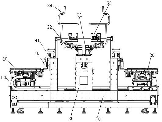
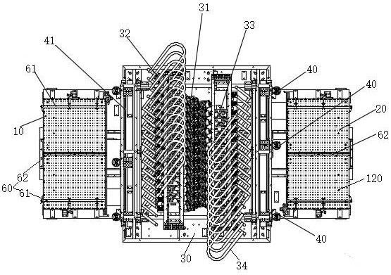
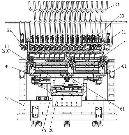
[0023] Please also refer to Figure 1 to Figure 3 ,...


PUM


Abstract

The invention provides a single-sided digital photoetching system. The single-sided digital photoetching system comprises a first platform, a second platform, a photoetching main body positioned between the first platform and the second platform, target point cameras arranged on two sides of the photoetching main body, and a transmission assembly for bearing the first platform and the second platform, the first platform and the second platform are both used for bearing a to-be-photoetched circuit board, the to-be-photoetched circuit board comprises a to-be-photoetched surface, and the transmission assembly is used for driving the first platform or the second platform to move towards the photoetched main body; and the target point camera is used for acquiring image information of a to-be-photoetched surface of the to-be-photoetched circuit board, so that the photoetching main body alternately performs digital photoetching treatment on the to-be-photoetched surface of the to-be-photoetched circuit board on the first platform and the second platform according to the image information. According to the single-sided digital photoetching system provided by the invention, the photoetching efficiency is improved, and the photoetching precision is improved.

Description

【Technical field】 [0001] The invention relates to the technical field of digital lithography of PCB boards, in particular to a single-sided digital lithography system of PCB boards. 【Background technique】 [0002] Photolithography technology refers to the technology of transferring the pattern on the mask plate to the substrate by means of photoresist (also known as photoresist) under the action of light. The main process is usually: first, ultraviolet light is irradiated on the surface of the substrate with a layer of photoresist film through the mask plate, causing the photoresist in the exposed area to undergo a chemical reaction, and then the exposed area or the unexposed area is dissolved and removed by developing technology. The photoresist (the former is called positive photoresist, the latter is called negative photoresist), so that the pattern on the mask plate is copied to the photoresist film, and finally the pattern is transferred to the substrate by etching tech...

Claims


Application Information

Patent Timeline
Patent Type & Authority Applications(China)
IPC IPC(8): G03F7/20
CPCY02P70/50
Inventor 陈志特王华甘泉龚海峰
Owner 广东科视光学技术股份有限公司
Why Eureka
Try Eureka