Price tag base station circuit and base station
A technology of price tag base station and base station, applied in the field of price tag base station circuit and base station, can solve the problems of slow download efficiency, affecting production and after-sales maintenance, etc., to achieve the effect of enhancing product strength, improving user experience, and ensuring reliability
- Summary
- Abstract
- Description
- Claims
- Application Information
AI Technical Summary
Problems solved by technology
Method used
Image
Examples
Embodiment 1
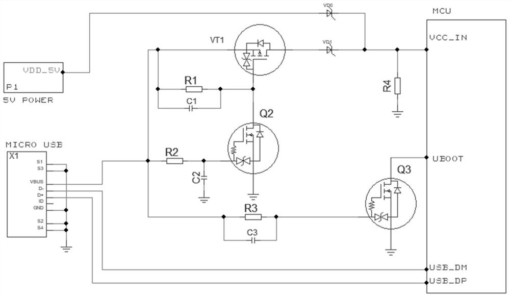
[0022] figure 1 It is the circuit diagram of the first embodiment of the price tag base station circuit of the present invention. This embodiment is a price tag base station circuit, which includes: system power supply VDD_5V, diode VD0, diode VD1, MCU power supply VCC_MCU, USB Vbus power supply, PMOS transistor VT1, NMOS transistor Q2, and NMOS transistor Q3. Wherein, the system power supply VDD_5V is connected to the anode of the diode VD0, and the cathode of the diode VD0 is connected to the MCU power supply VCC_MCU. The source of the PMOS transistor VT1 is connected to the USB Vbus power supply, the drain of the PMOS transistor VT1 is connected to the MCU power supply VCC_MCU through the diode VD1, and the control electrode of the PMOS transistor VT1 is connected to the source of the NMOS transistor Q2 Pole and connected in parallel with C1 through R1 to the USB Vbus power supply. The drain of the NMOS transistor Q2 is connected to the ground signal, and the control elec...
Embodiment 2
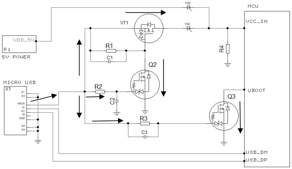
[0027] figure 2 It is the circuit diagram of the second embodiment of the price tag base station circuit of the present invention. Based on the above embodiment, when the system power supply VDD_5V is not powered, after the smart terminal is plugged into the USB cable, the USB Vbus power supply on the USB cable presents 5V Voltage, the 5V voltage of the USB Vbus power supply passes through the C3 capacitor to quickly boost the gate voltage of the NMOS transistor Q3 to 5V. When the gate voltage of the NMOS transistor Q3 starts to conduct during the rising process, when the voltage is turned on When it reaches the turn-on threshold, it is fully turned on, and the UBoot signal pin is a low-level signal.
[0028] In this embodiment, when the UBoot signal pin is a low-level signal, the 5V voltage of the USB Vbus power supply passes through the RC filter circuit R2C2, so that the gate voltage of the NMOS transistor Q2 is slowly boosted to 5V, so The gate voltage of the NMOS transi...
Embodiment 3
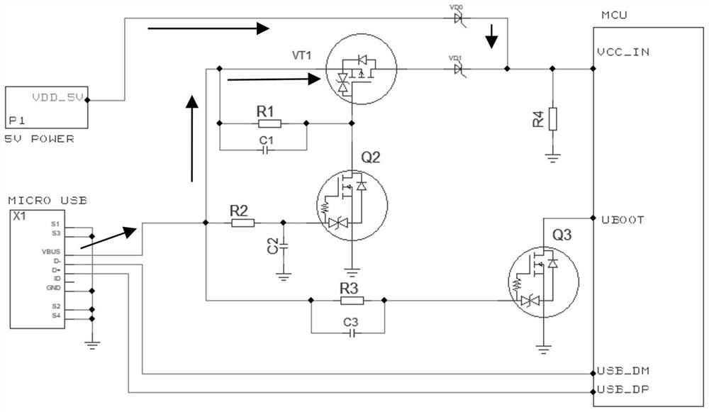
[0033] image 3 It is the circuit diagram of the third embodiment of the price tag base station circuit of the present invention. Based on the above embodiment, when the system power supply VDD_5V has been powered, after the smart terminal is plugged into the USB cable, the USB cable on the USB Vbus presents 5V voltage.
[0034] In this embodiment, the USB VBus 5V voltage passes through the C3 capacitor to quickly boost the gate voltage of the NMOS transistor Q3 to 5V. When the gate voltage of the NMOS transistor Q3 starts to conduct during the rising process, when the turn-on voltage reaches the turn-on When the threshold is fully turned on, the UBoot signal pin is a low level signal.
[0035] In this embodiment, when the UBoot signal pin is a low-level signal, the USB VBus 5V voltage passes through the RC filter circuit R2C2, so that the gate voltage of the NMOS transistor Q2 is slowly boosted to 5V, and the The gate voltage of the NMOS transistor Q2 starts to be turned on...
PUM
 Abstract
Description
Claims
Application Information
 - R&D Engineer
- R&D Manager
- IP Professional
- Industry Leading Data Capabilities
- Powerful AI technology
- Patent DNA Extraction
Browse by: Latest US Patents, China's latest patents, Technical Efficacy Thesaurus, Application Domain, Technology Topic, Popular Technical Reports.
© 2024 PatSnap. All rights reserved.Legal|Privacy policy|Modern Slavery Act Transparency Statement|Sitemap|About US| Contact US: help@patsnap.com


