Composite substrate structure and morphology improvement method thereof

A composite substrate and morphology technology, applied in the direction of electrical components, circuits, semiconductor devices, etc., can solve problems such as unfavorable tape-out processing, poor wafer morphology, etc., achieve good morphology, improve quality, and achieve high-quality Effect

Pending Publication Date: 2022-03-25
SHANGHAI NOVEL SI INTEGRATION TECH CO LTD
View PDF0 Cites 0 Cited by
  • Summary
  • Abstract
  • Description
  • Claims
  • Application Information

AI Technical Summary

Problems solved by technology

[0004] The technical problem to be solved by the present invention is that the wafer shape of the heterogeneous integrated substrate prepared by the prior art is poor, which is not conducive to the problem of subsequent tape-out processing

Method used


Image

  • Composite substrate structure and morphology improvement method thereof
  • Composite substrate structure and morphology improvement method thereof
  • Composite substrate structure and morphology improvement method thereof

Examples


Embodiment Construction

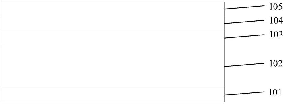
[0042] The technical solutions in the embodiments of the present application will be clearly and completely described below in conjunction with the drawings in the embodiments of the present application. Apparently, the described embodiments are only some of the embodiments of this application, not all of them. Based on the embodiments in this application, all other embodiments obtained by persons of ordinary skill in the art without creative efforts fall within the protection scope of this application.

[0043] Reference herein to "one embodiment" or "an embodiment" refers to a specific feature, structure or characteristic that may be included in at least one implementation of the present application. In the description of the present application, it should be understood that the orientation or positional relationship indicated by the terms "upper", "lower", "top", "bottom" etc. is based on the orientation or positional relationship shown in the drawings, and is only for It ...


PUM

PropertyMeasurementUnit
Thicknessaaaaaaaaaa
Thicknessaaaaaaaaaa
Stressaaaaaaaaaa

Abstract

The invention relates to the technical field of semiconductor material processing, in particular to a composite substrate structure and a morphology improvement method thereof. The structure comprises a first stress balance layer, a substrate layer, a second stress balance layer, a dielectric layer and a functional film layer which are arranged in sequence, the first stress balance layer and the second stress balance layer are made of the same material and are made of the same process; the first stress balance layer is used for adjusting the thickness of the first stress balance layer according to stress distribution in the composite substrate structure, so that the morphology of the composite substrate structure is improved; the second stress balance layer is used for balancing stress generated when the first stress balance layer is manufactured. In the composite substrate structure, the first stress balance layer is arranged on the back surface of the substrate layer and serves as the stress compensation layer, and when the heterogeneous integrated substrate is prepared, the wafer morphology is optimized by adjusting the thickness of the first stress balance layer, so that the overall morphology of the heterogeneous wafer can be more beneficial to subsequent tape-out processing.

Description

technical field [0001] The invention relates to the technical field of semiconductor material processing, in particular to a composite substrate structure and a method for improving its shape. Background technique [0002] With people's pursuit of increasing data transmission speed, performance, and power consumption of telecommunication equipment, the rapid development of chip technology has made it impossible for a single material to meet the needs of chip performance improvement and integration. People need to provide new chip integration solutions. Chip technology that achieves high performance, high integration and low power consumption. Combining multiple materials together to achieve heterogeneous integration of multiple materials has become an important path to improve chip performance and integration in the future. [0003] In the prior art, when manufacturing heterogeneous thin film material wafers, the heterogeneous materials are usually transferred, deposited, a...

Claims


Application Information

Patent Timeline
IPC IPC(8): H01L29/06H01L21/02
CPCH01L29/0684H01L21/02035
Inventor 欧欣陈阳黄凯
Owner SHANGHAI NOVEL SI INTEGRATION TECH CO LTD
Why Eureka
Try Eureka