Growth method for improving hole concentration of carbon-doped gallium indium arsenide
A technology of gallium indium arsenide and hole concentration, applied in chemical instruments and methods, crystal growth, single crystal growth, etc., can solve the problems of difficult film growth, poor controllability, and low activation rate, and achieve controllable Effects of growth, ease of control, and ease of doping concentration
- Summary
- Abstract
- Description
- Claims
- Application Information
AI Technical Summary
Problems solved by technology
Method used
Image

Examples
Embodiment 1
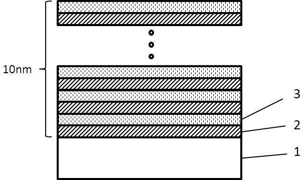
[0025] A growth method for increasing the hole concentration of carbon-doped gallium indium arsenide, using MBE technology for growth, such as figure 1 shown, including the following steps:
[0026] S1. Select an InP substrate, heat it to 350°C before growing, and bake for 30 minutes;
[0027] S2. Put the substrate into the growth chamber, and under the protection of P atmosphere, heat up to 520°C to remove the oxide film; quickly cool down to 480°C to grow an InP buffer layer of 500nm as the substrate 1, and then grow 0.47nm C-doped GaAs epitaxy Layer 2, where the doping concentration is 2E18cm -3 ;
[0028] S3. After growing the C-doped GaAs epitaxial layer 2, grow a 0.53nm non-doped InAs epitaxial layer 3 upward;
[0029] S4. Repeat step S3 and step S4 for a total of 10 cycles, grow 10nm in total, and drop to room temperature after the growth is completed; it is equivalent to growing a 10nm InGaAs extension layer on InP, wherein the first layer on InP is a C-doped GaAs e...
Embodiment 2
[0031] A growth method for increasing the hole concentration of carbon-doped gallium indium arsenide, using MBE technology for growth, comprising the following steps:
[0032] S1. Select an InP substrate, heat it to 350°C before growing, and bake for 30 minutes;
[0033] S2. Put the substrate into the growth chamber, and under the protection of P atmosphere, heat up to 520°C to remove the oxide film; quickly cool down to 480°C to grow an InP buffer layer of 500nm as the substrate 1, and then grow 0.3nm C-doped GaAs epitaxy Layer 2 with a concentration of 1E19cm -3 ;
[0034] S3. After growing the C-doped GaAs epitaxial layer 2, grow a 0.7nm non-doped InAs epitaxial layer 3;
[0035] S4. Repeat step S3 and step S4 for a total of 15 cycles, and grow 15nm in total; after the growth is completed, it is lowered to room temperature; it is equivalent to growing a 15nm InGaAs extension layer on InP, wherein the first layer on InP is a C-doped GaAs epitaxial layer 2. The uppermost l...
Embodiment 3
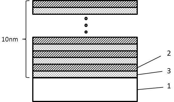
[0037] A growth method for increasing the hole concentration of carbon-doped gallium indium arsenide, using MBE technology for growth, such as figure 2 shown, including the following steps:
[0038] S1. Select an InP substrate, heat it to 350°C before growing, and bake for 30 minutes;
[0039] S2. Put the substrate into the growth chamber, and under the protection of P atmosphere, heat up to 520°C to remove the oxide film; rapidly cool down to 480°C to grow a 500nm InP buffer layer as the substrate 1, and then grow 0.47nm non-doped InAs epitaxy Layer 3;
[0040] S3. C-doped GaAs epitaxial layer 2 is grown upward with a thickness of 0.53nm, and the doping concentration is 2E18cm -3 ;
[0041] S4. Repeat step S2 and step S3 for a total of 10 cycles, and grow 10nm in total; after the growth is completed, drop to room temperature, which is equivalent to growing a 10nm InGaAs extension layer on InP, where the first layer on InP is a non-doped InAs epitaxial layer 3. The upperm...
PUM
| Property | Measurement | Unit |
|---|---|---|
| thickness | aaaaa | aaaaa |
Abstract
Description
Claims
Application Information
 - R&D
- Intellectual Property
- Life Sciences
- Materials
- Tech Scout
- Unparalleled Data Quality
- Higher Quality Content
- 60% Fewer Hallucinations
Browse by: Latest US Patents, China's latest patents, Technical Efficacy Thesaurus, Application Domain, Technology Topic, Popular Technical Reports.
© 2025 PatSnap. All rights reserved.Legal|Privacy policy|Modern Slavery Act Transparency Statement|Sitemap|About US| Contact US: help@patsnap.com