
Insulated gate bipolar transistor and manufacturing method thereof

A technology for bipolar transistors and manufacturing methods, which is applied in semiconductor/solid-state device manufacturing, semiconductor devices, electrical components, etc., can solve the problems of large threshold voltage influence, high equipment capability requirements, and poor process stability, and meets equipment capability requirements. Low, cost reduction, effect of reducing the influence of threshold voltage

Inactive Publication Date: 2022-03-08
SEMICON MFG ELECTRONICS (SHAOXING) CORP
View PDF4 Cites 0 Cited by
  • Summary
  • Abstract
  • Description
  • Claims
  • Application Information

AI Technical Summary

Problems solved by technology

At present, epitaxial or high-energy ion implantation methods are usually used to form the minority carrier storage layer. However, the process stability of these two methods is poor, the threshold voltage is greatly affected, and the requirements for equipment capabilities are high. Multi-layer epitaxy or high-energy ion implantation machines are required. High cost

Method used


Image

  • Insulated gate bipolar transistor and manufacturing method thereof
  • Insulated gate bipolar transistor and manufacturing method thereof
  • Insulated gate bipolar transistor and manufacturing method thereof

Examples


Embodiment Construction

[0039] In order to make the purpose, advantages and features of the present invention clearer, the insulated gate bipolar transistor and its manufacturing method proposed by the present invention will be further described in detail below. It should be noted that all the drawings are in a very simplified form and use imprecise scales, and are only used to facilitate and clearly assist the purpose of illustrating the embodiments of the present invention.

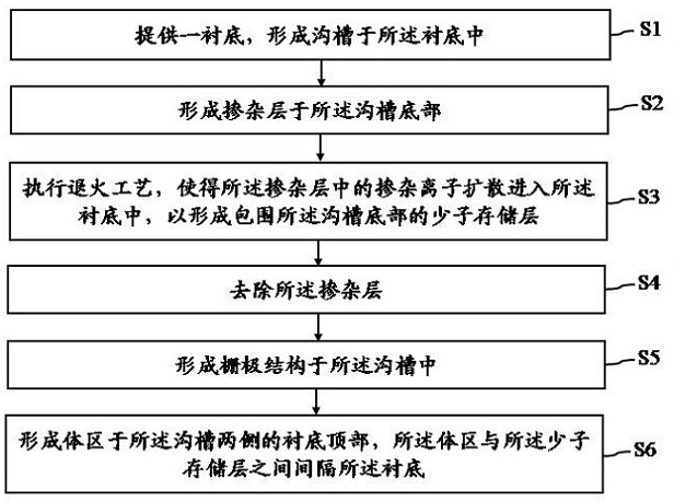
[0040] An embodiment of the present invention provides a method for manufacturing an insulated gate bipolar transistor, see figure 1 , figure 1 It is a flowchart of a method for manufacturing an insulated gate bipolar transistor according to an embodiment of the present invention, and the method for manufacturing an insulated gate bipolar transistor includes:

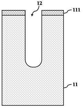
[0041] Step S1, providing a substrate, forming grooves in the substrate;

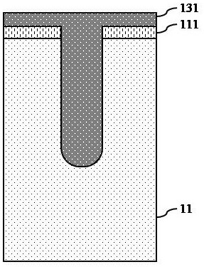
[0042] Step S2, forming a doped layer at the bottom of the trench;

[0043] Step S3, perfo...


PUM


Abstract

The invention provides an insulated gate bipolar transistor and a manufacturing method thereof, and the manufacturing method of the insulated gate bipolar transistor comprises the steps: providing a substrate, and forming a groove in the substrate; forming a doping layer at the bottom of the groove; an annealing process is executed, so that doped ions in the doped layer are diffused into the substrate, and a minority carrier storage layer surrounding the bottom of the groove is formed; the doping layer is removed; forming a gate structure in the trench; and forming a body region at the top of the substrate at two sides of the groove, and spacing the substrate between the body region and the minority carrier storage layer. According to the technical scheme, the influence on the threshold voltage can be reduced, and the cost is reduced.

Description

technical field [0001] The invention relates to the technical field of semiconductors, in particular to an insulated gate bipolar transistor and a manufacturing method thereof. Background technique [0002] IGBT (Insulated Gate Bipolar Transistor) is a device composed of MOSFET (input stage) and PNP transistor (output stage). It has the characteristics of easy driving, low input impedance and fast switching speed of MOSFET devices, and Bipolar devices have the advantages of large on-state current density, low on-state voltage, low loss, and good stability. [0003] The use of the minority carrier storage layer in the trench type IGBT can reduce its saturation voltage drop and turn-off time, which is beneficial to the improvement of device performance. At present, epitaxial or high-energy ion implantation methods are usually used to form the minority carrier storage layer. However, the process stability of these two methods is poor, the threshold voltage is greatly affected,...

Claims


Application Information

Patent Timeline
IPC IPC(8): H01L21/331H01L29/06H01L29/739
CPCH01L29/66068H01L29/66348H01L29/7398H01L29/7397H01L29/0684
Inventor 胡钰祺
Owner SEMICON MFG ELECTRONICS (SHAOXING) CORP
Learn More