Flash memory and forming method thereof
A memory and flash technology, applied in the field of flash memory and its formation, can solve problems such as poor performance of split-gate flash memory, and achieve the effects of improving erasing efficiency, reducing channel resistance and improving performance
- Summary
- Abstract
- Description
- Claims
- Application Information
AI Technical Summary
Problems solved by technology
Method used
Image

Examples
Embodiment Construction
[0030] As mentioned in the background, the performance of the prior art flash memory is poor.
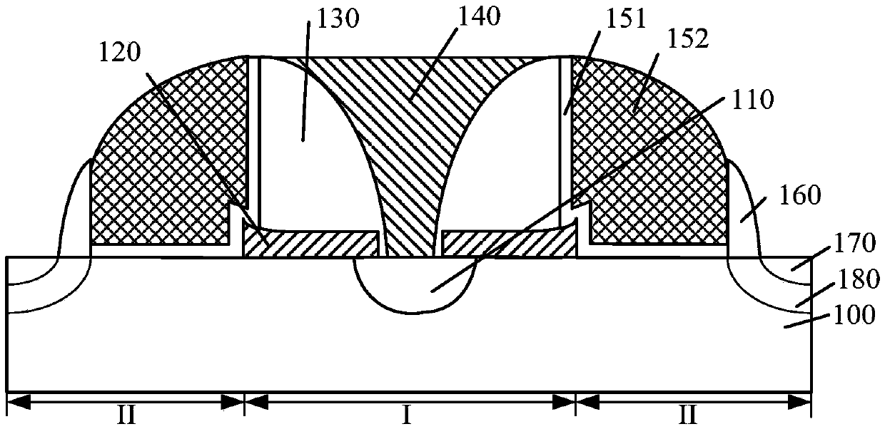
[0031] A structural schematic diagram of a flash memory, refer to figure 1 , including: a semiconductor substrate 100, the semiconductor substrate 100 includes a source line floating gate region I and a word line bit line region II, the source line floating gate region I is located between adjacent word line bit line regions II and Adjacent to the word line bit line region II; the floating gate structure 120 on the source line floating gate region I, the first spacer 130 on the floating gate structure 120, and the floating gate structure 120 and the first The source line layer 140 between the sidewalls 130; the source region 110 in the semiconductor substrate 100 located at the bottom of the source line layer 140; the word line structure located on the semiconductor substrate 100 in the word line bit line region II, the word line The line structure covers the sidewalls of the float...
PUM
 Abstract
Description
Claims
Application Information
 - R&D
- Intellectual Property
- Life Sciences
- Materials
- Tech Scout
- Unparalleled Data Quality
- Higher Quality Content
- 60% Fewer Hallucinations
Browse by: Latest US Patents, China's latest patents, Technical Efficacy Thesaurus, Application Domain, Technology Topic, Popular Technical Reports.
© 2025 PatSnap. All rights reserved.Legal|Privacy policy|Modern Slavery Act Transparency Statement|Sitemap|About US| Contact US: help@patsnap.com