


Quick Research
Generate reliable direction feasibility study reports for your R&D in just a few steps.

Technical Q&A
Discover and master advanced knowledge NOW. Basics, ideas, possibilities, all at once.

Find Solutions
As an expert in R&D theories, this can generate solutions to your technical problems instantly.

Evaluate Feasibility
Analyze your overall solution with one click, know your potential R&D risks in advance.

Monitor Landscape
Get weekly tech updates, stay abreast of the latest tech innovations and key insights.
Semiconductor device
A technology for semiconductors and devices, applied in the field of semiconductor devices using back gates, can solve problems such as difficult manufacturing processes, changes in the thickness of ultra-thin channels, and changes in threshold voltages
- Summary
- Abstract
- Description
- Claims
- Application Information
AI Technical Summary
Problems solved by technology
Method used
Image

Examples
no. 1 example
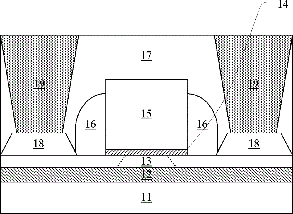
[0022] figure 1 A cross-sectional view showing a schematic structure of a semiconductor device according to the present invention. The semiconductor device includes source / drain regions formed in an ultra-thin semiconductor layer 13 and a channel region between the source / drain regions, and the interface between the source / drain regions and the channel region is indicated by a dotted line in the figure. A front gate stack is formed above the channel region, including a front gate dielectric layer 14 on the ultra-thin semiconductor layer 13 and a front gate 15 on the front gate dielectric layer 14 . Spacer walls 16 are formed on both sides of the front gate stack. A conductive channel 19 passing through the interlayer dielectric layer 17 and electrically contacting the source / drain region is formed above the source / drain region. A back gate dielectric layer 12 and a back gate 11 are formed under the ultrathin semiconductor layer 13 , wherein the back gate dielectric layer 12 ...
no. 2 example
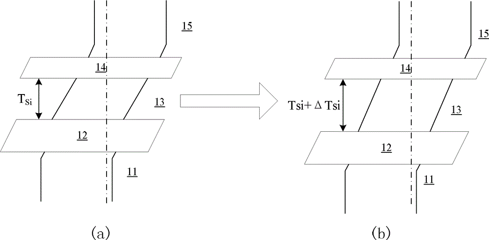
[0040] According to the second embodiment of the semiconductor device of the present invention, the front gate 15 and the back gate 11 are composed of the same material, and a forward bias voltage is applied to the front gate 15 and a forward bias voltage is applied to the back gate 11 during operation.
[0041] The thickness T of the ultra-thin semiconductor layer 13 Si When changing, this embodiment uses the forward bias voltage of the back gate 11 to change the surface potential φ calculated by the front gate 15 relative to the back gate 11 sp , so as to reduce or even completely cancel the influence of the thickness variation of the ultra-thin semiconductor layer 13 on the threshold voltage of the semiconductor device.
no. 3 example
[0043] According to the third embodiment of the semiconductor device of the present invention, the front gate 15 is made of high threshold voltage material, the back gate 11 is made of low threshold voltage material, and a forward bias voltage is applied to the front gate 15 during operation, and the back gate 11 is made of a material with a low threshold voltage. 11 Apply forward bias voltage.
[0044] The thickness T of the ultra-thin semiconductor layer 13 Si When changing, this embodiment not only utilizes the material combination of the front gate 15 and the back gate 11, but also uses the forward bias voltage of the back gate 11 to change the calculated surface potential φ of the front gate 15 relative to the back gate 11 sp , so as to reduce or even completely cancel the influence of the thickness variation of the ultra-thin semiconductor layer 13 on the threshold voltage of the semiconductor device.
PUM
 Abstract
Description
Claims
Application Information
 - R&D Engineer
- R&D Manager
- IP Professional
- Industry Leading Data Capabilities
- Powerful AI technology
- Patent DNA Extraction
Browse by: Latest US Patents, China's latest patents, Technical Efficacy Thesaurus, Application Domain, Technology Topic, Popular Technical Reports.
© 2024 PatSnap. All rights reserved.Legal|Privacy policy|Modern Slavery Act Transparency Statement|Sitemap|About US| Contact US: help@patsnap.com