Positioning processing method for scanning electron microscope shooting of silicon-based negative electrode material

A technology of silicon-based negative electrode materials and scanning electron microscopy, which is applied to the use of wave/particle radiation for material analysis, analysis of materials, circuits, etc., can solve the problems of affecting morphology observation, poor conductivity of silicon-based negative electrode materials, and poor conductivity. Prevent loose particles from floating, facilitate uniform export, and increase conductivity

Pending Publication Date: 2022-03-01
HEFEI GUOXUAN HIGH TECH POWER ENERGY
View PDF9 Cites 0 Cited by
  • Summary
  • Abstract
  • Description
  • Claims
  • Application Information

AI Technical Summary

Problems solved by technology

When observing samples with a scanning electron microscope, there are some problems with using a higher accelerating voltage (generally above 10kV): the electron beam has high energy and penetrates deeply into the sample, and what is obtained is not the real surface information of the sample; for samples that are not resistant to electron beams, such as organic Material damage is relatively large; for samples with poor conductivity, the accumulated charge on the surface causes charging and sample drift, which seriously affects the observation. The higher accelerating voltage provides relatively internal information rather than surface information, and cannot reflect the real surface. appearance
[0005] At present, scanning electron microscopes are used to shoot silicon-based negative electrode materials due to their poor conductivity and the easy expansion and looseness of particle volume. High-voltage secondary electrons are used to shoot.
In the high-voltage secondary electron mode, the electron beam has a certain penetration depth, and the resolution is low, which is not clear for the fine particle morphology.
In order to study the morphology information of the surface of the silicon-based negative electrode material itself, you can use the mode of low voltage acceleration and deceleration voltage to shoot, but in this mode, due to the poor conductivity of the silicon-based negative electrode material, the surface of the sample is easy to accumulate charges, resulting in charging and sample drift. Imaging showed severe long bright white areas (see Figure 4 ), which seriously affects the morphology observation

Method used


Image

  • Positioning processing method for scanning electron microscope shooting of silicon-based negative electrode material
  • Positioning processing method for scanning electron microscope shooting of silicon-based negative electrode material
  • Positioning processing method for scanning electron microscope shooting of silicon-based negative electrode material

Examples


Embodiment Construction

[0025] The following will clearly and completely describe the technical solutions in the embodiments of the present invention with reference to the accompanying drawings in the embodiments of the present invention. Obviously, the described embodiments are only some, not all, embodiments of the present invention. Based on the embodiments of the present invention, all other embodiments obtained by persons of ordinary skill in the art without making creative efforts belong to the protection scope of the present invention.

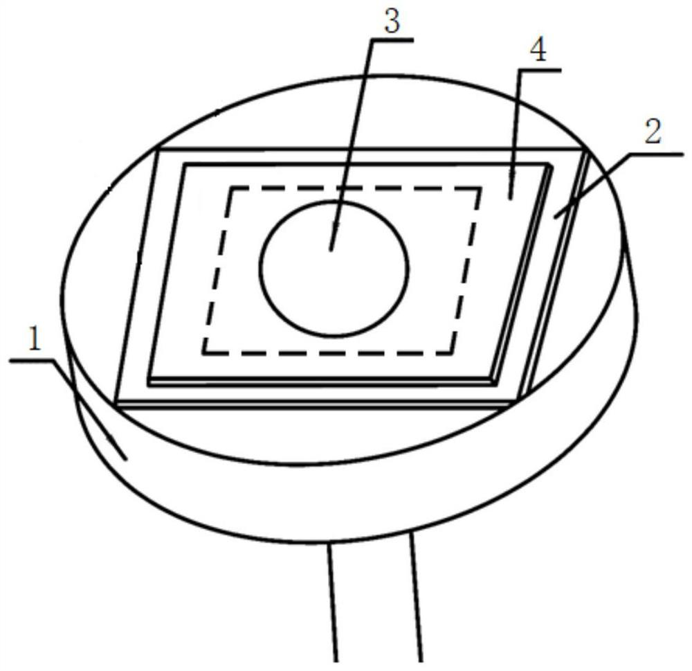
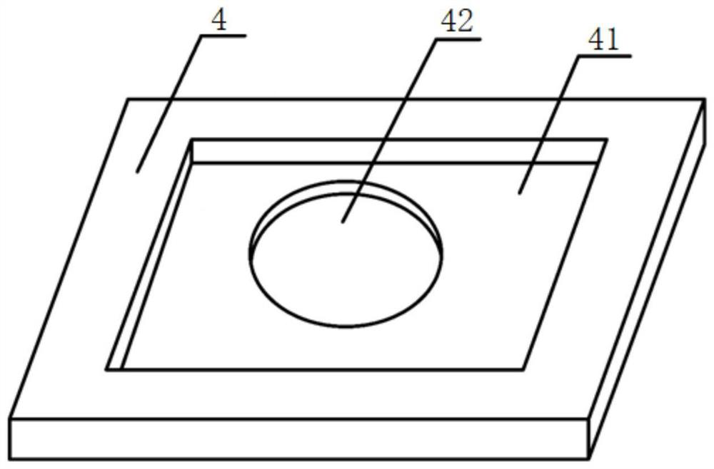
[0026] See figure 1 and figure 2 , a method for positioning and processing silicon-based negative electrode materials photographed by a scanning electron microscope, specifically comprising the following steps:

[0027] (1) Prepare the scissors, tweezers, latex gloves, dust-free cloth, ethanol reagent, ear cleaning ball, scanning electron microscope sample stage 1, double-sided conductive carbon tape 2, and the sample to be scanned of the silicon-based nega...


PUM

PropertyMeasurementUnit
thicknessaaaaaaaaaa
thicknessaaaaaaaaaa
thicknessaaaaaaaaaa

Abstract

The invention discloses a positioning treatment method for shooting a silicon-based negative electrode material by a scanning electron microscope, which comprises the following steps: firstly, adhering a double-sided conductive adhesive tape on a scanning electron microscope sample table, then adhering a to-be-scanned sample of the silicon-based negative electrode material to the upper surface of the double-sided conductive adhesive tape, and completely covering the double-sided conductive adhesive tape with the to-be-scanned sample; the double-sided conductive adhesive tape is arranged on the to-be-scanned sample, an unbonded annular area is reserved on the double-sided conductive adhesive tape, finally, a conductive edge sealing piece is fixed to the edge of the to-be-scanned sample, the conductive edge sealing piece seals the edge part of the to-be-scanned sample, and the conductive edge sealing piece is bonded to the periphery of the to-be-scanned sample and the unbonded annular area of the double-sided conductive adhesive tape. According to the method, a clear scanning electron microscope picture is obtained under the condition that the sample to be scanned is not damaged and the surface appearance of the sample to be scanned is not influenced, and a reliable basis is provided for analyzing the performance of a silicon-based negative electrode material.

Description

technical field [0001] The invention relates to the technical field of silicon-based negative electrode materials for lithium-ion batteries, in particular to a positioning processing method for scanning electron microscope photographing silicon-based negative electrode materials. Background technique [0002] Anode materials are one of the key factors determining the performance of lithium-ion batteries. Different anode materials can store lithium through intercalation, alloying, or conversion reactions. The current commercial negative electrode materials mainly include graphite (natural graphite and artificial graphite), amorphous carbon (soft carbon and hard carbon), lithium titanate and silicon-based materials (nano-silicon carbon materials, silicon oxide and amorphous silicon alloys). . Graphite has always been the most important anode material in the field of rechargeable lithium-ion batteries, and still occupies more than 95% of the market share. Compared with other ...

Claims


Application Information

Patent Timeline
Patent Type & Authority Applications(China)
IPC IPC(8): G01N23/2204G01N23/2251H01J37/20H01J37/28
CPCG01N23/2204G01N23/2251H01J37/20H01J37/28
Inventor 范海艳方婷婷胡淑婉张峥
Owner HEFEI GUOXUAN HIGH TECH POWER ENERGY
Why Eureka
Try Eureka