Eureka AIR delivers breakthrough ideas for toughest innovation challenges, trusted by R&D personnel around the world.

Electrostatic protection chip for quick charging management system and preparation method thereof

A management system and electrostatic protection technology, applied in the direction of circuits, diodes, electrical components, etc., can solve the problems of increased device area, large additional capacitance, and reduced device performance, so as to enhance withstand voltage performance, reduce parasitic capacitance, Effect of Reducing Leakage Current

Active Publication Date: 2022-01-14
深圳市金誉半导体股份有限公司
View PDF4 Cites 0 Cited by
  • Summary
  • Abstract
  • Description
  • Claims
  • Application Information

AI Technical Summary

Problems solved by technology

Usually, in order to improve the reverse characteristics of TVS, a guard ring structure and a metal field plate structure are used, but these two structures are easy to introduce large additional capacitance, and increase the device area, resulting in a decrease in the working performance of the device.

Method used


Image

  • Electrostatic protection chip for quick charging management system and preparation method thereof
  • Electrostatic protection chip for quick charging management system and preparation method thereof
  • Electrostatic protection chip for quick charging management system and preparation method thereof

Examples


Embodiment Construction

[0031] Embodiments of the present invention are described in detail below, examples of which are shown in the drawings, wherein the same or similar reference numerals designate the same or similar elements or elements having the same or similar functions throughout. The embodiments described below by referring to the figures are exemplary only for explaining the present invention and should not be construed as limiting the present invention.

[0032] It should be noted that when an element is referred to as being “fixed” to another element, it can be directly on the other element or there can also be an intervening element. When an element is referred to as being "connected to" another element, it can be directly connected to the other element or intervening elements may also be present. In contrast, when an element is referred to as being "directly on" another element, there are no intervening elements present. The terms "vertical," "horizontal," "left," "right," and similar...


PUM

PropertyMeasurementUnit
thicknessaaaaaaaaaa

Abstract

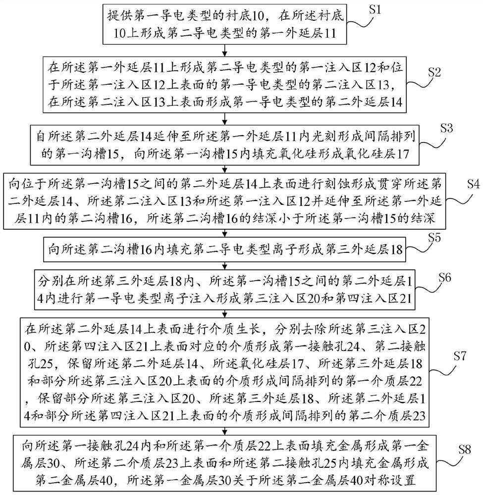
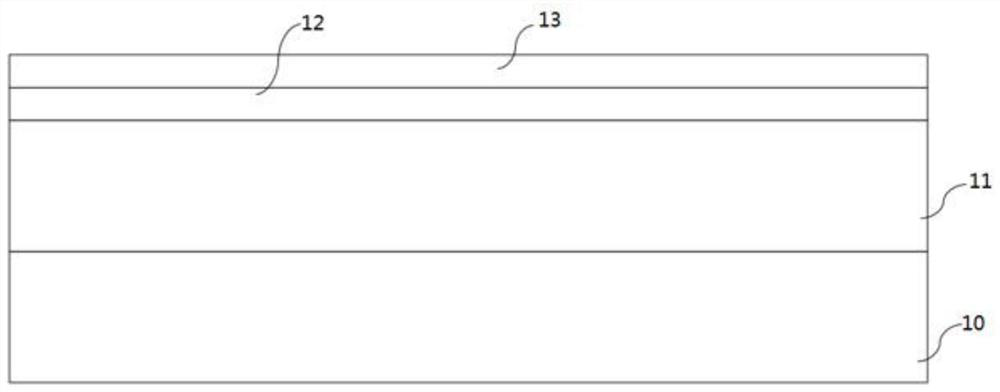
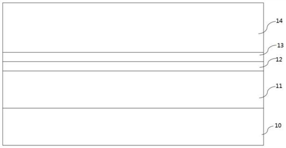
The invention discloses an electrostatic protection chip for a quick charge management system, which comprises a substrate, a first epitaxial layer formed on the substrate, a first injection region on the first epitaxial layer, a second injection region on the first injection region, a second epitaxial layer on the second injection region, first grooves extending into the first epitaxial layer from the second epitaxial layer and filled with silicon oxide layers, second grooves formed between the first grooves and filled with third epitaxial layers, third injection regions formed in the third epitaxial layers, a fourth injection region formed in the second epitaxial layer, a first dielectric layer, a second dielectric layer, a first contact hole and a second contact hole formed between the first dielectric layer and the second dielectric layer, and a first metal layer arranged in the first contact hole and on the first dielectric layer, and a second metal layer arranged on the second dielectric layer and in the second contact hole. The invention further provides a preparation method of the electrostatic protection chip for the quick charging management system, the discharge density is improved, and the manufacturing cost of the device is also reduced.

Description

technical field [0001] The invention belongs to the technical field of semiconductor chip manufacturing technology, and in particular relates to an electrostatic protection chip used in a fast charging management system and a preparation method thereof. Background technique [0002] As semiconductor devices are increasingly miniaturized, high-density, and multi-functional, electronic devices are increasingly vulnerable to voltage surges, which can even cause fatal injuries. Voltage surges ranging from electrostatic discharge to lightning can induce transient current spikes, and transient voltage suppressors (TVS) are often used to protect sensitive circuits from surges. Based on different applications, the transient voltage suppressor can protect the circuit by changing the surge discharge path and its own clamping voltage. [0003] The low-capacitance TVS structure is suitable for protection devices of high-frequency circuits, because it can reduce the interference of para...

Claims


Application Information

Patent Timeline
Patent Type & Authority Applications(China)
IPC IPC(8): H01L27/02H01L21/822
CPCH01L27/0296H01L27/0292H01L27/0255H01L21/822
Inventor 顾岚雁林河北胡慧雄
Owner 深圳市金誉半导体股份有限公司
Why Eureka
Eureka Blog
Learn More