
Broadband wave-absorbing metamaterial

A wave-absorbing material and broadband technology, which is applied in the field of broadband wave-absorbing superstructure materials, can solve the problems of narrow absorption frequency band, complex multi-layer structure design, and weak wave-absorbing ability, so as to reduce electromagnetic wave reflection and realize multifunctional structural integration , enhanced mechanical stability and environmental resistance

Pending Publication Date: 2021-12-31
NAT INNOVATION INST OF DEFENSE TECH PLA ACAD OF MILITARY SCI
View PDF0 Cites 8 Cited by
  • Summary
  • Abstract
  • Description
  • Claims
  • Application Information

AI Technical Summary

Problems solved by technology

[0005] The purpose of the present invention is to provide a broadband wave-absorbing superstructure, aiming at the difficulties faced by the existing wave-absorbing multi-phase materials and multilayer composite materials in terms of the difficulty in precise control of the dielectric parameters of the components and the complexity of the design of the multilayer structure. Solve the shortcomings of the current absorbing materials that need to be composed of two phases and the latter multi-phase, weak absorbing ability, narrow absorption frequency band, etc., and break through the existing design ideas of broadband absorbing structures based on multi-layer or sandwich structures, and provide broadband absorbing structures The design proposes a new design idea of ​​periodic structure

Method used


Image

  • Broadband wave-absorbing metamaterial
  • Broadband wave-absorbing metamaterial
  • Broadband wave-absorbing metamaterial

Examples


Embodiment 1

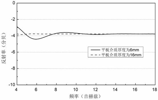
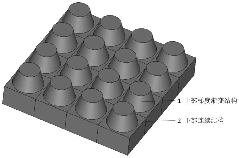
[0046] The cell unit period of the metamaterial is 12mm, the thickness of the upper part of the gradient structure is 8mm, the outline can be conical, and the radius of the bottom of the surface gradient structure gradually increases along the direction of electromagnetic wave incident propagation, and the thickness of the lower part of the continuum is 8mm , the total thickness is 16mm. The metamaterial uses a single dielectric absorbing medium with a dielectric constant of 5.56 and a loss tangent of 0.4. The ratio of top diameter to cell period area of ​​the upper gradient structure is 0.8, and the ratio of bottom diameter to cell period is 1.0. The reflectivity and effective absorptivity of periodic materials in the 4-18GHz wide frequency range are analyzed by finite element method, and the results are as follows figure 2 and image 3 shown. Depend on figure 2 It can be seen that the reflectivity of the periodic material is below -10dB in the wide frequency range of 4...

Embodiment 2

[0048] The dielectric constant of the metamaterial is 10, the loss tangent is 0.4, the thickness of the upper part of the gradient structure is 8mm, the shape is conical, and the radius of the bottom of the surface gradient structure increases gradually along the electromagnetic wave incident propagation direction, and the lower part is continuous The thickness of the medium is 8mm, and the total thickness is 16mm. The broadband reflection and absorbing properties of materials under two periodic structures were simulated and analyzed. One is that the cell period is 14mm, and the diameter of the gradient structure at the upper part of the electromagnetic wave incident end is 9.8mm, that is, the ratio of it to the period is 0.7; the other is that The cell period is 10mm, and the diameter of the gradient structure at the incident end of the upper part of the electromagnetic wave is 6.0mm, that is, the ratio of it to the period is 0.6. The result is as follows Figure 6 and Figu...

Embodiment 3

[0050] The dielectric constant of the metamaterial is 10, the loss tangent is 0.4, the thickness of the upper part of the gradient structure is 8 mm, and the outline is parabolic, and the radius of the bottom of the surface gradient structure increases gradually along the direction of electromagnetic wave incident propagation. Its shape is as follows: Figure 8 shown. The thickness of the lower part of the continuum is 10mm, and the total thickness is 18mm. The cell period is 14mm, and the diameter of the gradient structure at the incident end of the upper part of the electromagnetic wave is 5.6mm, that is, the ratio of it to the period is 0.4. The broadband reflection and absorbing performance of the metamaterial is simulated and analyzed, and the results are as follows Figure 9 and Figure 10 shown. It can be seen that the reflectivity of the periodic medium is below -10dB in the wide frequency range of 4-18 GHz, which can effectively reduce the reflection of the detectio...


PUM

PropertyMeasurementUnit
Thicknessaaaaaaaaaa
Thicknessaaaaaaaaaa
Thicknessaaaaaaaaaa

Abstract

The invention belongs to the technical field of wave-absorbing materials and metamaterials, and provides a broadband wave-absorbing metamaterial comprising periodically arranged cellular units, the periodic distribution of the cellular units is square, and the period size is determined according to the wave absorbing bandwidth and the highest wave absorbing working frequency, so that obvious diffraction and reflection of electromagnetic waves on the surface of a material are avoided. The cellular unit is made of a single medium type wave-absorbing medium, the cellular unit is divided into an upper part and a lower part along the incident propagation direction of electromagnetic waves, the upper part is of an axisymmetric gradient gradual change structure, and the lower part is of a continuous structure; and the thicknesses of the upper and lower dielectric parts of the cell are determined according to the wave-absorbing bandwidth, the intrinsic dielectric constant of the dielectric wave-absorbing material and the loss angle tangent value. The characteristic that the dielectric constant of the material gradually changes along with the thickness can be controlled by designing the change gradients of different outlines, so that surface reflection is reduced as much as possible, electromagnetic waves effectively enter the wave-absorbing material, and loss is continuously absorbed in the propagation process.

Description

technical field [0001] The invention belongs to the technical field of wave-absorbing materials and metamaterials, and in particular relates to a broadband wave-absorbing metamaterial. Background technique [0002] Electromagnetic absorbing materials that are lightweight, resistant to environmental corrosion and strong absorbing are the key materials for equipment stealth. How to reduce the reflection coefficient and broaden the absorbing bandwidth is the key to the development of new absorbing materials. Generally, absorbing materials need to have both impedance matching characteristics and loss characteristics to convert electromagnetic wave energy into heat energy and dissipate it. The impedance matching characteristic refers to the matching of the surface impedance value of the absorbing material with the impedance value of the electromagnetic wave, so that the reflectivity of the surface is the lowest, allowing as much electromagnetic waves as possible to enter the inte...

Claims


Application Information

Patent Timeline
IPC IPC(8): H01Q15/00H01Q17/00
CPCH01Q17/00H01Q15/0086
Inventor 邹春荣郭少军沈同圣周晓松
Owner NAT INNOVATION INST OF DEFENSE TECH PLA ACAD OF MILITARY SCI
Learn More