Manufacturing method of semiconductor chip and laser

A manufacturing method and semiconductor technology, applied in the laser field, can solve the problems of reducing the luminous efficiency of the laser, reducing the working efficiency of the device, reducing the light absorption, etc., and achieving the effects of improving the anti-COD ability, improving the production efficiency, and shortening the diffusion time.

Pending Publication Date: 2021-12-10
SHENZHEN LASER INST
View PDF0 Cites 1 Cited by
  • Summary
  • Abstract
  • Description
  • Claims
  • Application Information

AI Technical Summary

Problems solved by technology

[0003] At present, the mainstream method used to increase the COD threshold is to reduce the light absorption of the cavity surface. The basic method is to increase the bandgap width of the cavity surface area, which is often referred to as the window structure. The specific implementation methods include the following: one is epitaxial regrowth, After etching away the material near the cavity surface, re-epitaxially grow a wide bandgap material to form a transparent window for output light and reduce light absorption. The disadvantage is that the process is more complicated, the cost is higher, and it may lead to poor crystal quality at the junction. and the device's working efficiency is reduced, thereby affecting the performance of the device; the second is quantum well hybridization, because each layer of the epitaxial wafer is a metastable interface, so through quantum hybridization technology, the quantum well component atoms in the cavity surface region will diffuse each other , thus increasing the bandgap width of the corresponding non-window region
[0004] However, the problem that existing zinc atom diffusion increases the bandgap width of the window region is that although it takes a short time (about 30 minutes) for zinc atoms to diffuse into the quantum well layer, due to the thickness of the quantum well layer being about 10nm, relying solely on It takes 1 to 3 hours for zinc to induce atomic mixing, so the total doping time is long, which is not conducive to process production; in addition, doping needs to be carried out in a high-temperature environment, and long-term high-temperature treatment will increase the lateral or Longitudinal diffusion, which seriously affects the atomic purity of the active region and reduces the luminous efficiency of the laser

Method used


Image

  • Manufacturing method of semiconductor chip and laser
  • Manufacturing method of semiconductor chip and laser
  • Manufacturing method of semiconductor chip and laser

Examples


Embodiment Construction

[0020] The following will clearly and completely describe the technical solutions in the embodiments of the present application with reference to the drawings in the embodiments of the present application. Obviously, the described embodiments are only some of the embodiments of the present application, not all of them. Based on the embodiments in this application, all other embodiments obtained by persons of ordinary skill in the art without making creative efforts belong to the scope of protection of this application.

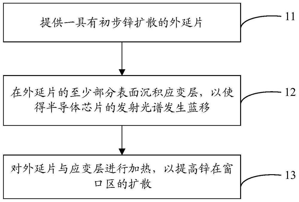
[0021] Please refer to Figure 1 to Figure 3 , figure 1 It is a schematic flow chart of an embodiment of a method for manufacturing a semiconductor chip provided by the present application, the method comprising:

[0022] Step 11: Providing an epitaxial wafer with preliminary zinc diffusion.

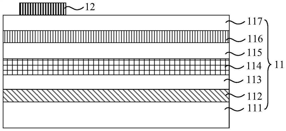
[0023] like figure 2 As shown, the epitaxial wafer 11 includes an N-type substrate 111, an N-type cladding layer 112, a first waveguide layer 113, a quantum well lay...


PUM

PropertyMeasurementUnit
thicknessaaaaaaaaaa
thicknessaaaaaaaaaa
thicknessaaaaaaaaaa

Abstract

The invention discloses a manufacturing method of a semiconductor chip and a laser. The method comprises the steps of providing an epitaxial wafer with preliminary zinc diffusion; depositing a strain layer on at least part of the surface of the epitaxial wafer so as to enable blue shift of the emission spectrum of the semiconductor chip to occur, wherein at least part of the surface comprises a window area; and heating the epitaxial wafer and the strain layer to improve the diffusion of zinc in the window area, wherein the film strain of the strain layer after heating is greater than the film strain before heating. Through the mode, diffusion of zinc can be accelerated, the production efficiency is improved, and the capability of resisting catastrophic optical mirror surface damage is improved.

Description

technical field [0001] The present application relates to the field of laser technology, in particular to a method for manufacturing a semiconductor chip and a laser. Background technique [0002] The research focus of semiconductor lasers includes increasing optical output power, improving reliability and working life, etc. Catastrophic Optical Damage (COD, Catastrophic Optical Damage) is an important factor affecting the maximum output power and reliability of semiconductor lasers. [0003] At present, the mainstream method used to increase the COD threshold is to reduce the light absorption of the cavity surface. The basic method is to increase the bandgap width of the cavity surface area, which is often referred to as the window structure. The specific implementation methods include the following: one is epitaxial regrowth, After etching away the material near the cavity surface, re-epitaxially grow a wide bandgap material to form a transparent window for output light an...

Claims


Application Information

Patent Timeline
Patent Type & Authority Applications(China)
IPC IPC(8): H01S5/02257H01S5/028
CPCH01S5/028H01S2304/04
Inventor 郑兆祯吴阳烽焦旺王菊廖桂波丁新琪涂庆明
Owner SHENZHEN LASER INST
Why Eureka
Try Eureka