Inspection apparatus adjustment system and inspection apparatus adjustment method
A technology for inspecting devices and adjusting systems, applied to measuring devices, image enhancement, instruments, etc., can solve problems such as reducing wafer production efficiency
- Summary
- Abstract
- Description
- Claims
- Application Information
AI Technical Summary
Problems solved by technology
Method used
Image
Examples
Embodiment 1
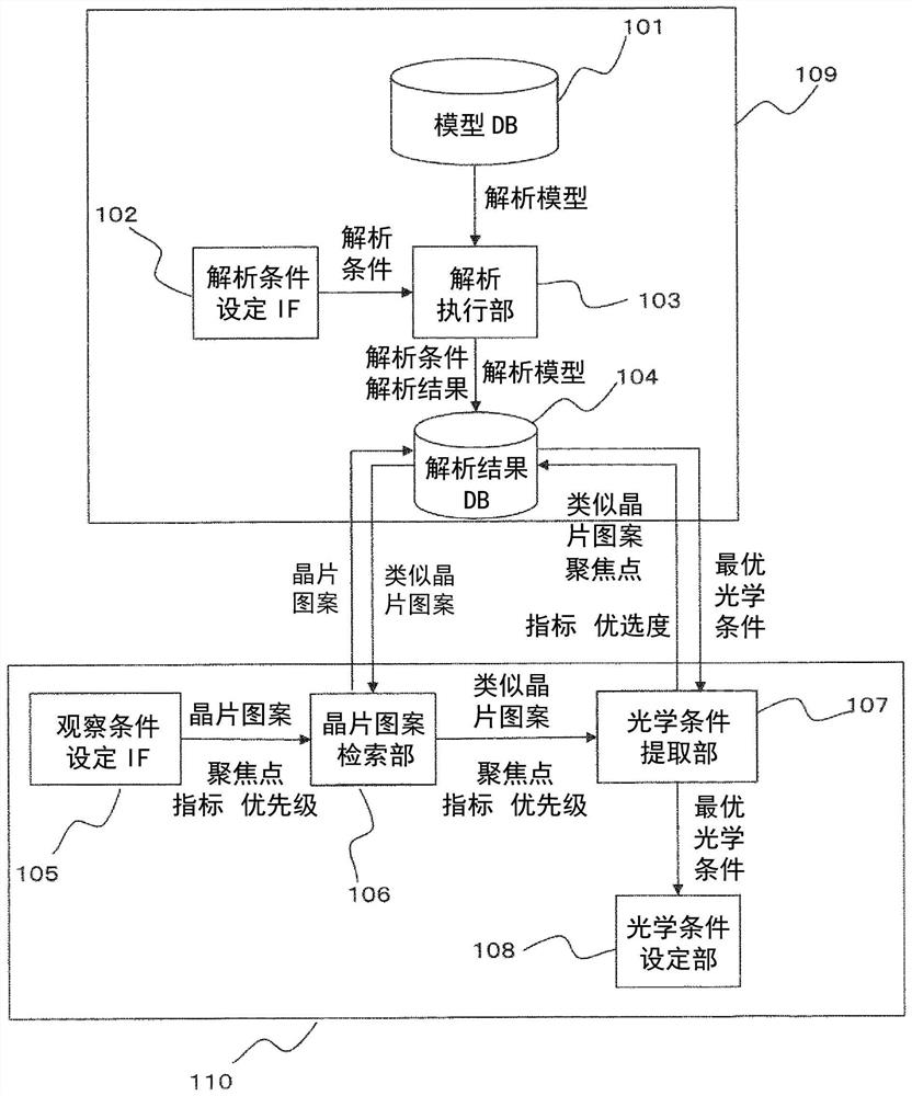
[0031] exist figure 1 The inspection device automatic adjustment system according to the first embodiment is shown. The inspection device automatic adjustment system includes a model DB 101 , an analysis condition setting IF 102 , an analysis execution unit 103 , an analysis result DB 104 , an observation condition setting IF 105 , a wafer pattern search unit 106 , an optical condition extraction unit 107 , and an optical condition setting unit 108 . The model DB 101, the analysis condition setting IF 102, the analysis execution unit 103, and the analysis result DB 104 are used as the analysis result DB creation unit 109, and the observation condition setting IF 105, the wafer pattern search unit 106, the optical condition extraction unit 107, and the optical condition setting unit 108 serves as an optimal optical condition extraction unit 110 .
[0032] The configuration of the analysis result DB creation unit 109 will be described. In the analysis result DB creation part 1...
Embodiment 2
[0056] Next, in Figure 9 The inspection device automatic adjustment system according to the second embodiment is shown. In Embodiment 2, the analysis result DB creation unit 109 is connected to various devices and databases via the network 901 . Furthermore, the specification can be received via the network 901, or the analysis result DB 104 can be shared among a plurality of inspection devices. In other words, cloudification of the analysis result DB creating unit 109 is realized.
[0057] For example, suppose that after delivery of the inspection apparatus, the optical conditions need to be re-set even when the specifications of the inspected wafers are greatly different, but there is no wafer model in the model DB. Therefore, the analysis result DB creation unit 109 of the inspection device automatic adjustment system is built in a PC within the inspection device manufacturer, and the optimal optical condition extraction unit 110 is installed in the inspection device bod...
Embodiment 3
[0060] exist Figure 10 show Figure 8 Additional examples of extraction methods for optimal optical conditions are shown. This is an extraction flow of optimal optical conditions assuming the case of measuring the width of the bottom of a deep hole. In order to measure the width with high precision, it is necessary to focus on the bottom, but in actual wafers, the depth may vary. The processing performed in the optical condition extraction unit 107 to solve this will be described below.
[0061]First, an estimated value of the depth deviation is set (step 1001). This is set based on past performance values and information from customers. For example, the difference between the actual depth performance value in past inspections input via the observation condition setting IF 105 and the depth included in the information from the customer is calculated and used as an estimated value.
[0062] Next, an optimal optical condition obtained from an analytical model (wafer mode...
PUM
 Abstract
Description
Claims
Application Information
 - R&D Engineer
- R&D Manager
- IP Professional
- Industry Leading Data Capabilities
- Powerful AI technology
- Patent DNA Extraction
Browse by: Latest US Patents, China's latest patents, Technical Efficacy Thesaurus, Application Domain, Technology Topic, Popular Technical Reports.
© 2024 PatSnap. All rights reserved.Legal|Privacy policy|Modern Slavery Act Transparency Statement|Sitemap|About US| Contact US: help@patsnap.com


