A Low Voltage High Linearity Cascode Amplifier
A common source amplifier, common gate amplifier technology, used in amplifiers, amplifiers with semiconductor devices/discharge tubes, improving amplifiers to reduce nonlinear distortion, etc. Guarantee the circuit amplification state and other issues, to achieve the effect of enhancing the maximum power output capability, avoiding performance loss, and ensuring normal working conditions
- Summary
- Abstract
- Description
- Claims
- Application Information
AI Technical Summary
Problems solved by technology
Method used
Image
Examples
Embodiment 1
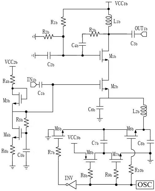
[0076] This embodiment proposes a low-voltage high-linearity cascode amplifier, including a Cascode amplifier and a voltage boosting unit;
[0077] The Cascode amplifier comprises a cascaded common-source amplifier and a common-gate amplifier; the NMOS transistor M used as a common-source transistor is arranged in the described common-source amplifier 1b , the NMOS transistor M used as a common-gate transistor is arranged in the common-gate amplifier 2b ; The NMOS transistor M 2b Drain with NMOS transistor M 1b source connection; the NMOS transistor M 2b The source of is connected to the voltage boosting unit.
[0078] Working principle: through the voltage boost unit, the NMOS transistor M in the Cascode amplifier unit is improved 1b The potential difference between the drain and the source of the NMOS transistor M2b enhances the output voltage swing and maximum power output capability of the Cascode amplifier unit, thereby effectively improving the linearity of the casco...
Embodiment 2
[0080] On the basis of the above-mentioned embodiment 1, in order to better realize the present invention, this embodiment further includes a DC bias unit connected to the gate of the NMOS transistor M2b.
[0081] Working principle: The DC bias unit provides a stable DC operating point for the Cascode amplifier unit in the full temperature range (-55°C to 125°C), avoiding the performance loss caused by the drift of the DC operating point.
[0082] Other parts of this embodiment are the same as those of Embodiment 1 above, so details are not repeated here.
Embodiment 3
[0084] On the basis of any one of the above-mentioned embodiments 1-2, in order to better realize the present invention, this embodiment further includes a DC separation unit, and the DC separation unit is arranged between the Cascode amplifier and the voltage boosting unit During this period, the source of the NMOS transistor M2b in the Cascode amplifier is first connected to the DC separation unit, and then connected to the voltage boosting unit through the DC separation unit.
[0085] Working principle: The DC separation unit ensures that the voltage boost unit does not affect the electrical characteristics of the Cascode amplifier unit, and ensures that the low-voltage and high-linearity cascode amplifier is in normal working condition.
[0086] Other parts of this embodiment are the same as those of any one of Embodiments 1-2 above, so details are not repeated here.
PUM
 Abstract
Description
Claims
Application Information
 - R&D
- Intellectual Property
- Life Sciences
- Materials
- Tech Scout
- Unparalleled Data Quality
- Higher Quality Content
- 60% Fewer Hallucinations
Browse by: Latest US Patents, China's latest patents, Technical Efficacy Thesaurus, Application Domain, Technology Topic, Popular Technical Reports.
© 2025 PatSnap. All rights reserved.Legal|Privacy policy|Modern Slavery Act Transparency Statement|Sitemap|About US| Contact US: help@patsnap.com


