Mini LED backlight source, backlight module and manufacturing method of Mini LED backlight source
A technology of backlight and LED chips, which is applied in the fields of optics, nonlinear optics, semiconductor/solid-state device manufacturing, etc., can solve the problems of small size, large number of chips, and great influence of module effect, so as to increase the light-emitting angle and change the space Distributing and improving the effect of uniformity
- Summary
- Abstract
- Description
- Claims
- Application Information
AI Technical Summary
Problems solved by technology
Method used
Image
Examples
Embodiment 1
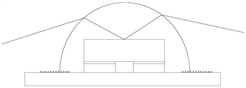
[0029] This embodiment discloses a Mini LED backlight; including:
[0030] Substrate 100, the material of substrate in this example is FR4 plate, and substrate surface has a plurality of welding areas (single welding area such as 102 / 1021), is provided with one deck light-reflecting layer 101 to cover outside welding area, and in this embodiment, reflective The material of the layer is a mixture of silicone resin and TiO2.
[0031] The surface of the reflective layer on the side away from the substrate (that is, the side of the reflective layer combined with the encapsulation layer) has a microstructure of 50 um.
[0032] The flip-chip LED chip 104, the size of the flip-chip LED chip in this embodiment is 200um*400um, the dominant wavelength is 450nm, and the bottom of each flip-chip LED chip has a first electrode and a second electrode. The flip-chip LED chip is arranged above the soldering area of the substrate.
[0033] A plurality of metal connection layers 103 / 1031, w...
Embodiment 2
[0039] This embodiment discloses a Mini LED backlight. The difference between it and Embodiment 1 is that the material of the substrate is a BT board, and there are two reflective layers in total. The reflective layer in contact with the substrate is an epoxy resin reflective layer. The surface of the resin reflective layer covers the second reflective layer, the second reflective layer is a silicon rubber reflective layer, and there is a 30um microstructure on the surface of the second reflective layer away from the substrate, the size of the chip in this embodiment is 100*200um, A light-reflecting layer structure 108 is covered on the light-emitting surface of the chip. In this embodiment, the arrangement of the chips on the substrate is a polygonal arrangement ( Figure 5 right). In this embodiment, a is 0.1 mm, b is 0.01 mm, b / 2a=0.05; in this embodiment, the material of the encapsulation layer is silicone rubber.
[0040] The preparation method of the Mini LED backlight ...
Embodiment 3
[0042] This embodiment discloses a Mini LED backlight. The difference between it and Embodiment 1 is that in this embodiment, the material of the encapsulation layer is epoxy resin, and the encapsulation layer also contains nanoparticles. In this embodiment, the nanoparticles are SiO2, a is 0.5mm, b is 0.5mm, b / 2a=0.5.
PUM
 Abstract
Description
Claims
Application Information
 - R&D
- Intellectual Property
- Life Sciences
- Materials
- Tech Scout
- Unparalleled Data Quality
- Higher Quality Content
- 60% Fewer Hallucinations
Browse by: Latest US Patents, China's latest patents, Technical Efficacy Thesaurus, Application Domain, Technology Topic, Popular Technical Reports.
© 2025 PatSnap. All rights reserved.Legal|Privacy policy|Modern Slavery Act Transparency Statement|Sitemap|About US| Contact US: help@patsnap.com


