A kind of semiconductor growth equipment and working method thereof

A semiconductor and equipment technology, applied in the field of semiconductor growth equipment, can solve the problems of high optimal growth temperature range and narrow use range, and achieve the effect of reducing the growth temperature range and expanding the use range

Active Publication Date: 2022-02-01
SUZHOU EVERBRIGHT PHOTONICS CO LTD +1
View PDF10 Cites 0 Cited by
  • Summary
  • Abstract
  • Description
  • Claims
  • Application Information

AI Technical Summary

Problems solved by technology

[0004] Therefore, the technical problem to be solved by the present invention is to overcome the problems of high optimum growth temperature range and narrow application range of semiconductor growth equipment in the prior art, thereby providing a semiconductor growth equipment and its working method

Method used


Image

  • A kind of semiconductor growth equipment and working method thereof
  • A kind of semiconductor growth equipment and working method thereof
  • A kind of semiconductor growth equipment and working method thereof

Examples


Embodiment Construction

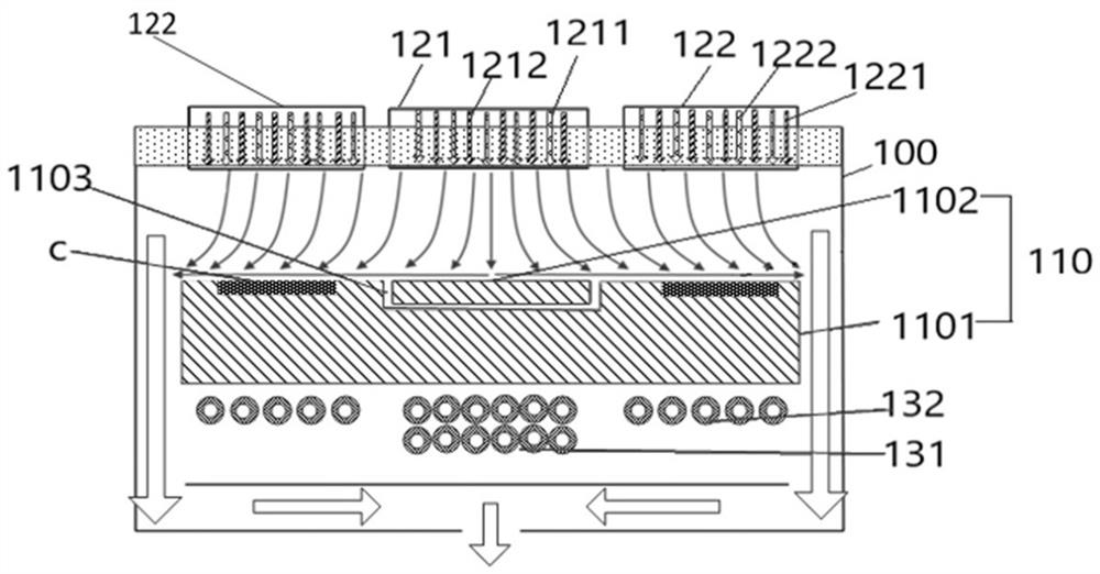
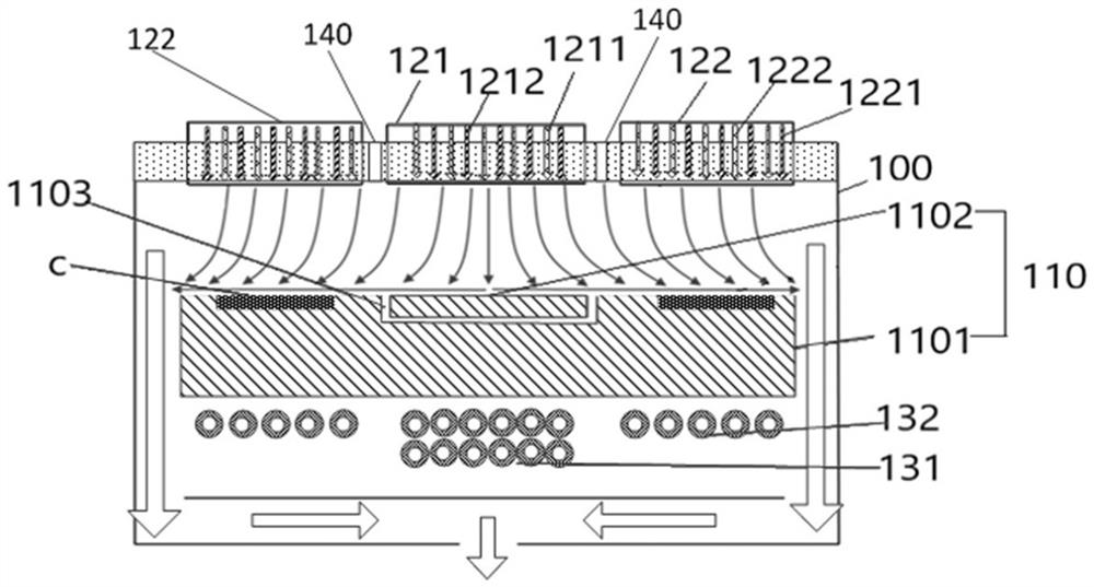
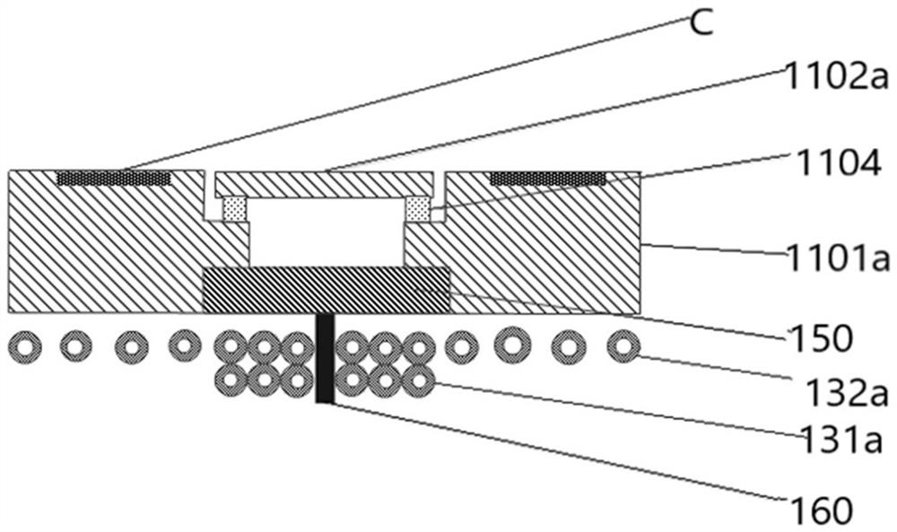
[0038] There are three main types of MOCVD reaction chambers, which are planetary air cushion rotating horizontal reaction chambers, high-speed rotating disk reaction chambers, and close-coupled spray reaction chambers.

[0039] In the planetary air cushion rotating horizontal reaction chamber, when the Group III reaction gas source and the Group V reaction gas source are used, the Group III reaction gas source and the Group V reaction gas source enter the reaction chamber from the three-laminar flow nozzle on the upper cover respectively, and pass through the grid The grid is forced to turn and flow radially to the outer edge horizontally along the 360-degree annular space between the base on which the substrate is placed and the ceiling, and flows out through the perforated quartz side ring. The base is a graphite base and the ceiling is a quartz ceiling. or graphite canopy. This flow pattern eliminates the sidewalls of the horizontal reaction chamber and therefore sidewall ...


PUM


Abstract

The invention provides a semiconductor growth device and its working method. The semiconductor growth device includes: a reaction chamber; a heating base located in the reaction chamber, the heating base includes a first heating area and a The second heating zone, the heating temperature of the first heating zone is greater than the heating temperature of the second heating zone, the surface of the second heating zone is suitable for placing the substrate; the first spraying unit and the second spraying unit at the top of the reaction chamber unit, the first spray unit is located above the first heating zone, and the second spray unit is located above the second heating zone; the first spray unit at least includes a first pipeline, and the first pipeline is suitable for passing into the second heating zone. A gas source, the second spray unit at least includes a second pipeline, the second pipeline is suitable for passing into the second gas source, the decomposition temperature of the first gas source is higher than the decomposition temperature of the second gas source. The optimal growth temperature range of the semiconductor growth equipment is reduced, and the application range is expanded.

Description

technical field [0001] The invention relates to the technical field of semiconductors, in particular to a semiconductor growth device and a working method thereof. Background technique [0002] Semiconductor devices such as semiconductor lasers, high electron mobility transistors, photodetectors, etc. are often produced by epitaxial growth technology, and the two most common epitaxial technologies are metal-organic chemical vapor deposition (MOCVD) and molecular beam epitaxy (MBE). . Compared with MBE, MOCVD is more suitable for large-scale commercial production due to its advantages of good growth stability, easy maintenance, and high output. In recent years, its market share has been increasing year by year. Although MOCVD has the above advantages over MBE, the optimum growth temperature range of the semiconductor growth equipment used by MOCVD is significantly higher than that used by MBE. Therefore, many materials that need to be grown at low temperatures cannot be grow...

Claims


Application Information

Patent Timeline
Patent Type & Authority Patents(China)
IPC IPC(8): C23C16/46C23C16/455C23C16/52C23C16/30H01L21/02H01L21/67
CPCC23C16/46C23C16/45565C23C16/45574C23C16/52C23C16/301H01L21/0262H01L21/67017H01L21/67103C23C16/4581C23C16/4584
Inventor 王俊程洋肖啸郭银涛苟于单
Owner SUZHOU EVERBRIGHT PHOTONICS CO LTD
Why Eureka
Try Eureka