WIFI dual-band band-stop frequency selective surface
A frequency-selective surface, dual-band technology, applied to waveguide devices, electrical components, circuits, etc., can solve problems such as increased power consumption
- Summary
- Abstract
- Description
- Claims
- Application Information
AI Technical Summary
Problems solved by technology
Method used
Image
Examples
Embodiment Construction
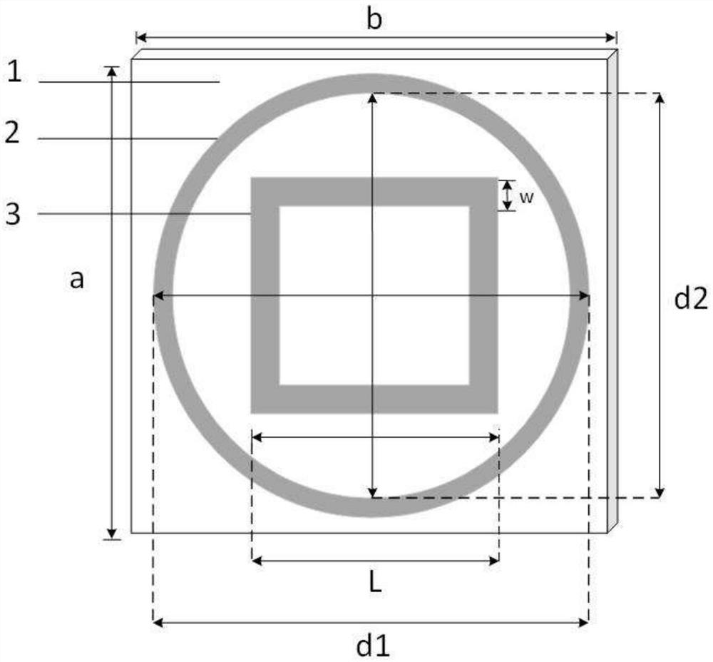
[0013] Such as Figure 4 As shown, the frequency selective surface of this embodiment is composed of several identical unit structure periodic arrangements, such as figure 1 As shown, each unit structure includes a dielectric substrate, a metal layer arranged on the front of the dielectric substrate; the metal layer includes a circular patch, and a square ring patch arranged in the circular patch; the medium The centers of the substrate, the circular patch, and the square ring patch are coincident.
[0014] The material of the metal layer is copper; the outer diameter d1 of the circular patch is 26.0712mm, and the inner diameter d2 is 24.8024mm; the length L of the outer side of the square ring patch is 16.0724mm, and its line width W is 2.0039mm.
[0015] The length and width of the dielectric substrate are both 28.0013 mm, and the thickness is 1.0192 mm. The material used is FR-4, and the relative dielectric constant is 4.3.
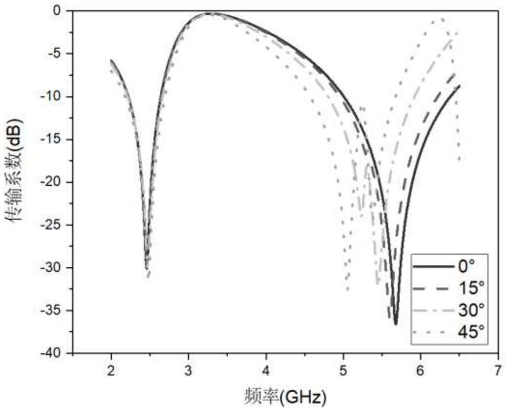
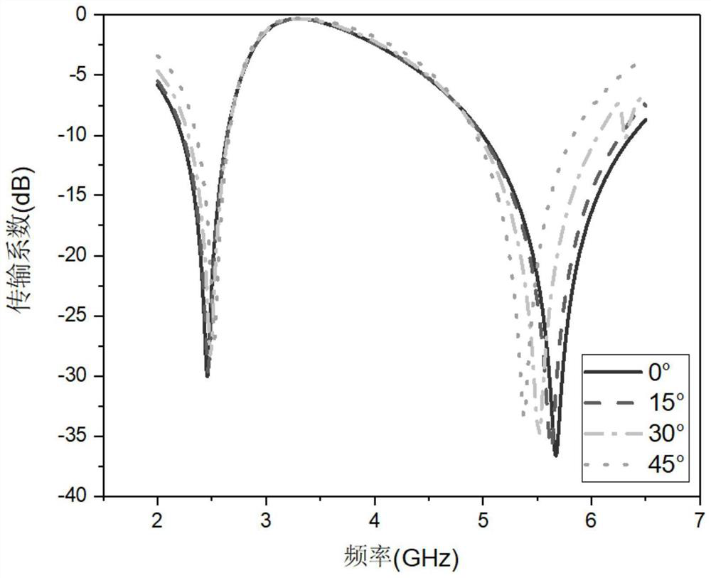
[0016] From figure 2 , image 3 It can be s...
PUM
| Property | Measurement | Unit |
|---|---|---|
| Thickness | aaaaa | aaaaa |
| Outer diameter | aaaaa | aaaaa |
| Inner diameter | aaaaa | aaaaa |
Abstract
Description
Claims
Application Information
 - R&D
- Intellectual Property
- Life Sciences
- Materials
- Tech Scout
- Unparalleled Data Quality
- Higher Quality Content
- 60% Fewer Hallucinations
Browse by: Latest US Patents, China's latest patents, Technical Efficacy Thesaurus, Application Domain, Technology Topic, Popular Technical Reports.
© 2025 PatSnap. All rights reserved.Legal|Privacy policy|Modern Slavery Act Transparency Statement|Sitemap|About US| Contact US: help@patsnap.com


