goa circuit and its electrical aging test method

A kind of aging test and circuit technology, applied in the direction of electronic circuit test, measurement power, measurement device, etc., can solve the problem of poor stability of GOA circuit, and achieve the effect of reducing production cost, increasing production capacity and improving efficiency

Active Publication Date: 2022-07-12
TCL CHINA STAR OPTOELECTRONICS TECH CO LTD
View PDF0 Cites 0 Cited by
  • Summary
  • Abstract
  • Description
  • Claims
  • Application Information

AI Technical Summary

Problems solved by technology

[0006] The object of the present invention is to provide a GOA circuit and its electrical aging test method to solve the technical problem of poor stability of the GOA circuit

Method used


Image

  • goa circuit and its electrical aging test method
  • goa circuit and its electrical aging test method
  • goa circuit and its electrical aging test method

Examples


Embodiment 2

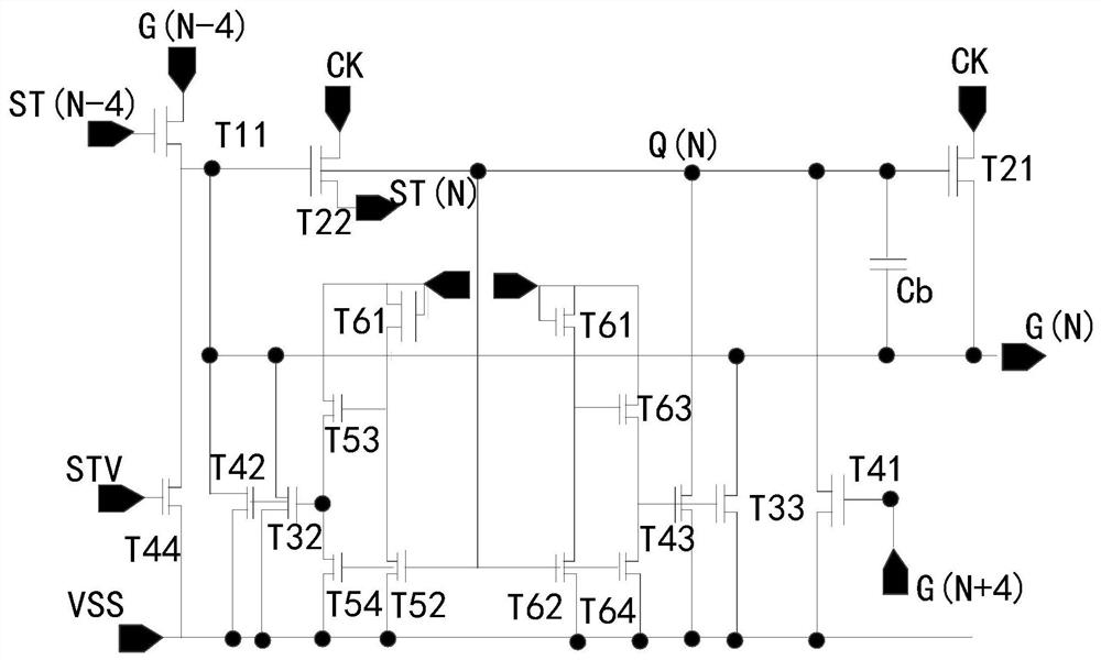
[0065] This embodiment provides a GOA circuit and an electrical aging test method thereof, including most of the technical features of Embodiment 1, the difference is that when the GOA circuit performs an electrical aging test, the first constant voltage low level is set The voltage difference between the voltage of the signal VSSQ and the second constant voltage low level signal VSSG is greater than 0, so that the first thin film transistor T11, the second thin film transistor T21 and the third thin film transistor T22 are electrically aged .

[0066] When the GOA circuit is subjected to an electrical aging test, when the first thin film transistor T11, the second thin film transistor T21 and the third thin film transistor T22 are all P-type thin film transistors, the first constant voltage low power The voltage difference between the voltage of the level signal VSSQ and the second constant-voltage low-level signal VSSG is greater than 0, which is mainly to make the thin film...


PUM


Abstract

The present application discloses a GOA circuit and an electrical aging test method thereof. The GOA circuit includes a plurality of cascaded GOA structural units, and the Nth-level GOA unit includes: a first thin film transistor, a second thin film transistor, a third thin film transistor, a first thin film transistor, and a third thin film transistor. Four thin film transistors and a fifth thin film transistor; the first thin film transistor is connected to the pull-up control signal and the gate signal, and the first thin film transistor, the fifth thin film transistor, the second thin film transistor and the third thin film transistor are connected to the first node; Both the second thin film transistor and the third thin film transistor are connected to the clock signal, and the third thin film transistor outputs a pull-up control signal; the fourth thin film transistor is connected to the second constant voltage low level signal and the fifth thin film transistor is connected to the first constant voltage low level signal. The present invention sets the voltage difference between the voltage of the first constant voltage low level signal and the second constant voltage low level signal to be greater than 0 or less than 0, so that the first thin film transistor, the second thin film transistor and the third thin film transistor are electrically aged .

Description

technical field [0001] The present application relates to the field of display technology, and in particular, to a GOA circuit and an electrical aging test method thereof. Background technique [0002] The basic concept of GOA (Gate Driver on Array, array substrate row drive technology) circuit is to integrate the gate drive circuit of a TFT-LCD (thin film transistor-liquid crystal display, thin film transistor liquid crystal display) panel (referred to as a liquid crystal panel) on a glass surface. On the substrate, the scanning drive for the liquid crystal panel is formed. Compared with the traditional driving technology using COF (Chip On Flex, or, Chip On Film, often called chip on film), GOA circuit can greatly save the manufacturing cost, and save the Bonding process of COF on the Gate (gate) side ( Binding process), which is also extremely beneficial to productivity improvement. Therefore, GOA is a key technology for the development of LCD panels in the future. [...

Claims


Application Information

Patent Timeline
Patent Type & Authority Patents(China)
IPC IPC(8): G09G3/36G01R31/28
CPCG09G3/006G09G3/3677G01R31/2849
Inventor 吕晓文袁驰文
Owner TCL CHINA STAR OPTOELECTRONICS TECH CO LTD
Why Eureka
Try Eureka