Long-wave infrared multispectral imaging device based on filter array and design method of device
A multi-spectral imaging and long-wave infrared technology, applied in the field of multi-spectral imaging, can solve problems such as inability to perform real-time imaging structures, unfavorable system miniaturization and integration, and complexity, and achieve simple structure, high integration, and simple structural form Effect
- Summary
- Abstract
- Description
- Claims
- Application Information
AI Technical Summary
Problems solved by technology
Method used
Image
Examples
Embodiment 1
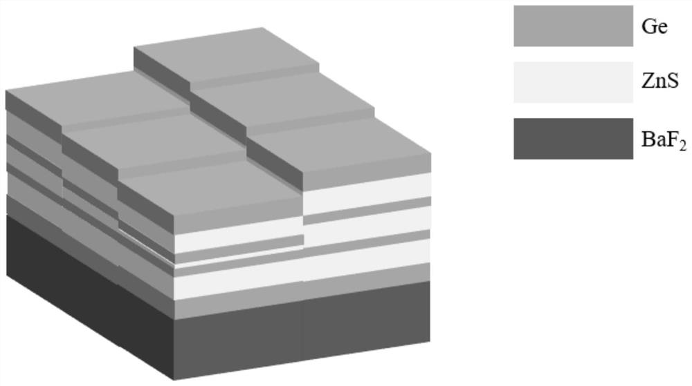
[0064] In this embodiment, a 6-channel multi-spectral imaging device is designed for incident light signals in the long-wave infrared band with a wavelength range of 8.00-12.00 μm, and the 2×3 filter array structure is as follows figure 1 As shown, the size of each multilayer film structure matches the pixel size of the detector used, and the side length is 25.00 μm.
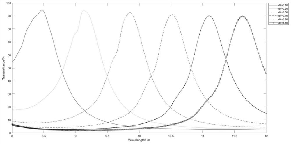
[0065] Using the above method, the CST software is used for parameter scanning and combined with the calculation of the transfer matrix method to optimize the material, number of layers and thickness of each film layer of the multilayer film structure. Specifically, the substrate of the multilayer film structure is BaF with thickness d=1.00mm 2 , the number of multilayer films is 7 layers, which is composed of 4 layers of Ge and 3 layers of ZnS alternately arranged, and the thickness is d 1 = 0.80 μm, d 2 = 1.00 μm, d 3 = 0.36 μm, d 4 、d 5 = 0.36 μm, d 6 = 1.00 μm, d 7 = 0.80 μm. Changing the thickness d...
Embodiment 2
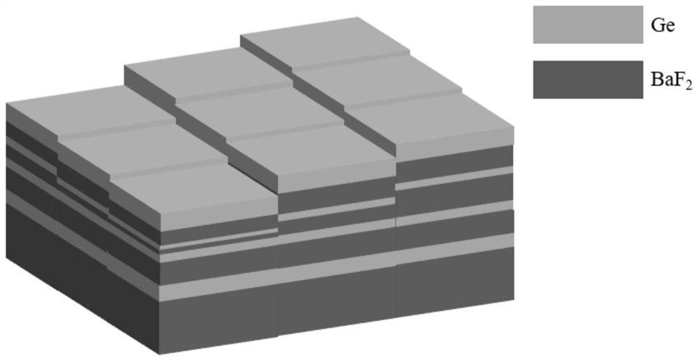
[0069]In this embodiment, a 9-channel multi-spectral imaging device is designed for incident light signals in the long-wave infrared band with a wavelength range of 8.00 to 12.00 μm, in which the 3×3 filter array is as image 3 As shown, the size of each multilayer film structure matches the pixel size of the detector used, and the side length is 25.00 μm.
[0070] Using the above method, the CST software is used to scan parameters and combine with the calculation of the transfer matrix method to optimize the material, number of layers and thickness of each film layer of the multilayer film. Specifically, the substrate of the multilayer film structure is BaF with thickness d=1.00mm 2 , the number of layers of the multilayer film is 7 layers, consisting of 4 layers of Ge and 3 layers of BaF 2 Alternately arranged, the thickness is d 1 = 0.70 μm, d 2 = 1.10 μm, d 3 = 0.40 μm, d 4 、d 5 = 0.40 μm, d 6 = 1.10 μm, d 7 = 0.70 μm. Change the middle layer BaF 2 Thickness d 4...
Embodiment 3
[0074] In this embodiment, a 4-channel multi-spectral imaging device is designed for incident light signals in the long-wave infrared band with a wavelength range of 8.00-12.00 μm, in which the 2×2 filter array is as Figure 5 As shown, the size of each multilayer film structure matches the pixel size of the detector used, and the side length is 25.00 μm.
[0075] Using the above method, the CST software is used to scan parameters and combine with the calculation of the transfer matrix method to optimize the material, number of layers and thickness of each film layer of the multilayer film. Specifically, the substrate of the multilayer film structure is BaF with thickness d=1.00mm 2 , the number of layers of the multilayer film is 5 layers, consisting of 3 layers of Ge and 2 layers of BaF 2 Alternately arranged, the thickness is d 1 = 0.50 μm, d 2 = 0.80 μm, d 3 、d 4 = 0.80 μm, d 5 = 0.50 μm. Changing the thickness d of the interlayer Ge 3 The central wavelength of tra...
PUM
| Property | Measurement | Unit |
|---|---|---|
| wavelength | aaaaa | aaaaa |
| thickness | aaaaa | aaaaa |
| thickness | aaaaa | aaaaa |
Abstract
Description
Claims
Application Information
 - R&D
- Intellectual Property
- Life Sciences
- Materials
- Tech Scout
- Unparalleled Data Quality
- Higher Quality Content
- 60% Fewer Hallucinations
Browse by: Latest US Patents, China's latest patents, Technical Efficacy Thesaurus, Application Domain, Technology Topic, Popular Technical Reports.
© 2025 PatSnap. All rights reserved.Legal|Privacy policy|Modern Slavery Act Transparency Statement|Sitemap|About US| Contact US: help@patsnap.com


