MOSFET chip manufacturing method for improving grid characteristics
A manufacturing method and chip technology, applied in semiconductor/solid-state device manufacturing, electrical components, transistors, etc., can solve problems such as the inability to effectively limit the current flowing through the gate, save space, reduce switching losses, and improve discharge efficiency. Effect
- Summary
- Abstract
- Description
- Claims
- Application Information
AI Technical Summary
Problems solved by technology
Method used
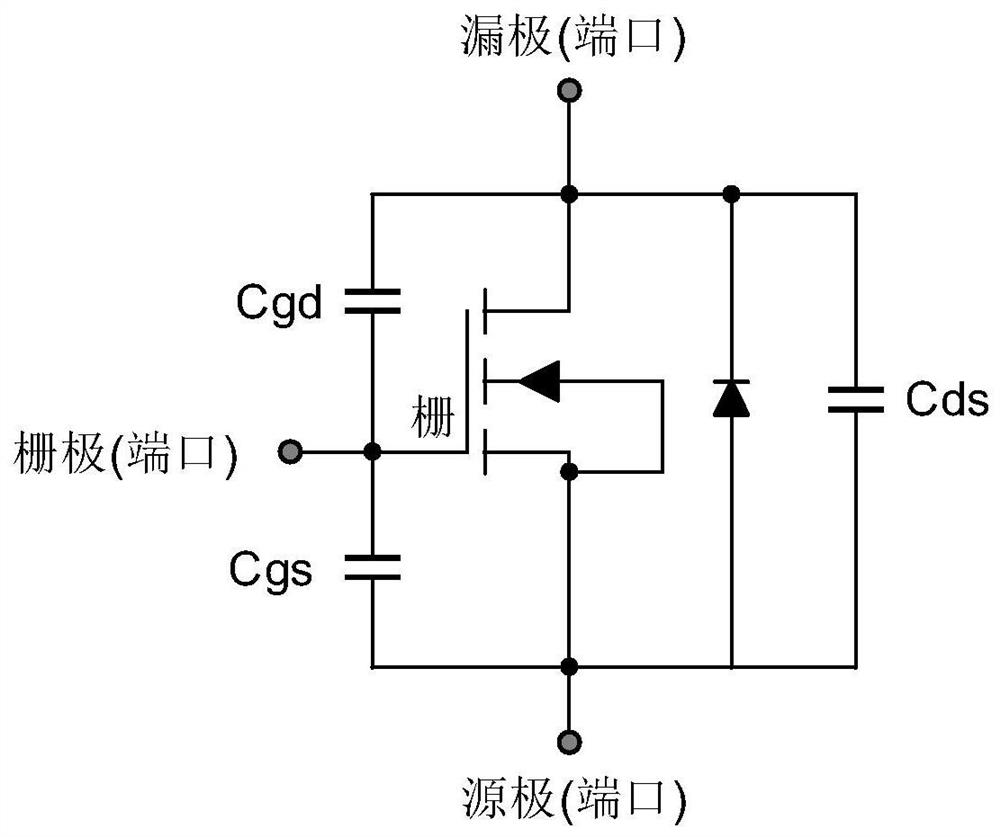
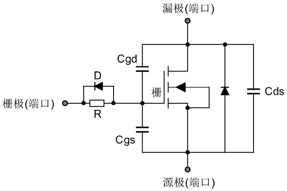
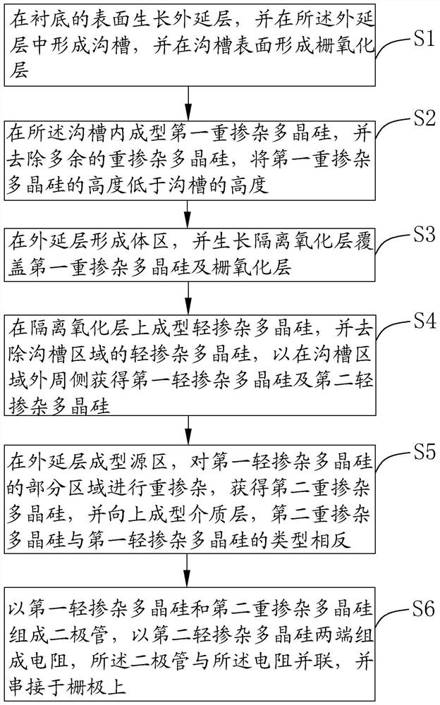
Image

Examples
Embodiment Construction
[0042] The following will clearly and completely describe the technical solutions in the embodiments of the present invention with reference to the accompanying drawings in the embodiments of the present invention. Obviously, the described embodiments are some of the embodiments of the present invention, but not all of them. Based on the embodiments of the present invention, all other embodiments obtained by persons of ordinary skill in the art without making creative efforts belong to the protection scope of the present invention.
[0043] It should also be understood that the terminology used in the description of the present invention is for the purpose of describing particular embodiments only and is not intended to be limiting of the present invention. As used in this specification and the appended claims, the singular forms "a", "an" and "the" are intended to include plural referents unless the context clearly dictates otherwise.
[0044] It should also be further unders...
PUM
 Abstract
Description
Claims
Application Information
 - R&D
- Intellectual Property
- Life Sciences
- Materials
- Tech Scout
- Unparalleled Data Quality
- Higher Quality Content
- 60% Fewer Hallucinations
Browse by: Latest US Patents, China's latest patents, Technical Efficacy Thesaurus, Application Domain, Technology Topic, Popular Technical Reports.
© 2025 PatSnap. All rights reserved.Legal|Privacy policy|Modern Slavery Act Transparency Statement|Sitemap|About US| Contact US: help@patsnap.com