Low noise amplifier and base station radio frequency front end
A low-noise amplifier and port technology, applied in the field of radio frequency front-end, can solve the problems of alternating distortion and adjacent channel interference in the working system of the base station, and achieve the effect of improving intermodulation distortion and adjacent channel interference and high linearity.
- Summary
- Abstract
- Description
- Claims
- Application Information
AI Technical Summary
Problems solved by technology
Method used
Image
Examples
Embodiment 1
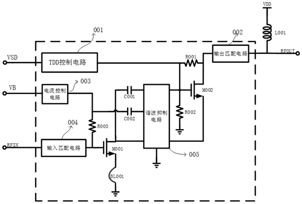
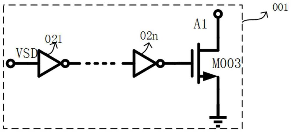
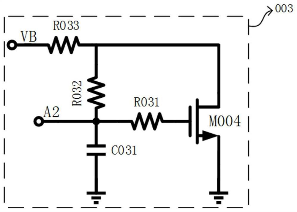
[0022] The low noise amplifier in this embodiment specifically includes a TTD control circuit 001, an output matching circuit 002, a current control circuit 003, an input matching circuit 004, a first-stage transistor M001, a second-stage transistor M002, a feedback circuit and a harmonic suppression circuit 005. One end of the TTD control circuit 001 is connected to the control port VSD, the other end is connected to one end of the resistor R001, one end of the resistor R002, one end of the second-stage transistor M002, and one end of the harmonic suppression circuit 005, and the other end of the resistor R001 is connected to the first The second terminal of the secondary transistor M002 is connected to one terminal of the output matching circuit 002, the other terminal of the output matching circuit 002 is connected to the output port RFOUT, and the third terminal of the second-stage transistor M002 is connected to the second terminal of the harmonic suppression circuit 005 O...
Embodiment 2
[0024] Please refer to figure 1 as shown, figure 1 The structural block diagram of the low noise amplifier provided by the embodiment of the present invention.
[0025] The low noise amplifier in this embodiment specifically includes a TTD control circuit 001, an output matching circuit 002, a current control circuit 003, an input matching circuit 004, a first-stage transistor M001, a second-stage transistor M002, a feedback circuit and a harmonic suppression circuit 005. One end of the TTD control circuit 001 is connected to the control port VSD, the other end is connected to one end of the resistor R001, one end of the resistor R002, one end of the second-stage transistor M002, and one end of the harmonic suppression circuit 005, and the other end of the resistor R001 is connected to the first The second terminal of the secondary transistor M002 is connected to one terminal of the output matching circuit 002, the other terminal of the output matching circuit 002 is connecte...
Embodiment 3
[0031] Please refer to Figure 4 as shown, Figure 4 The structural block diagram of the low noise amplifier provided by the embodiment of the present invention.
[0032] The low noise amplifier in this embodiment specifically includes a TTD control circuit 001, an output matching circuit 002, a current control circuit 003, an input matching circuit 004, a first-stage transistor M001, a second-stage transistor M002, a feedback circuit and a harmonic suppression circuit 005. One end of the TTD control circuit 001 is connected to the control port VSD, the other end is connected to one end of the resistor R001, one end of the resistor R002, one end of the second-stage transistor M002, and one end of the harmonic suppression circuit 005, and the other end of the resistor R001 is connected to the first The second terminal of the secondary transistor M002 is connected to one terminal of the output matching circuit 002, the other terminal of the output matching circuit 002 is connec...
PUM
 Abstract
Description
Claims
Application Information
 - Generate Ideas
- Intellectual Property
- Life Sciences
- Materials
- Tech Scout
- Unparalleled Data Quality
- Higher Quality Content
- 60% Fewer Hallucinations
Browse by: Latest US Patents, China's latest patents, Technical Efficacy Thesaurus, Application Domain, Technology Topic, Popular Technical Reports.
© 2025 PatSnap. All rights reserved.Legal|Privacy policy|Modern Slavery Act Transparency Statement|Sitemap|About US| Contact US: help@patsnap.com


