Infrared sensor chip and manufacturing method based on semiconductor double-gate transistor structure

A dual-gate transistor, infrared sensor technology, used in semiconductor devices, final product manufacturing, sustainable manufacturing/processing, etc., can solve problems such as low detection sensitivity

Active Publication Date: 2021-12-21
西安中科立德红外科技有限公司
View PDF8 Cites 0 Cited by
  • Summary
  • Abstract
  • Description
  • Claims
  • Application Information

AI Technical Summary

Problems solved by technology

[0003] However, the detection sensitivity of the semiconductor infrared sensor chip of the related art to the intensity of infrared light is on the low side. Therefore, a semiconductor infrared sensor chip with higher detection sensitivity is required.

Method used


Image

  • Infrared sensor chip and manufacturing method based on semiconductor double-gate transistor structure
  • Infrared sensor chip and manufacturing method based on semiconductor double-gate transistor structure
  • Infrared sensor chip and manufacturing method based on semiconductor double-gate transistor structure

Examples


Embodiment Construction

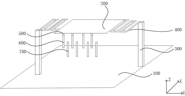
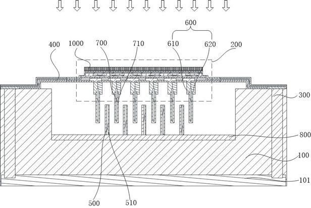
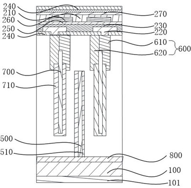
[0060] In the related art, the semiconductor infrared sensor chip has the problem of insensitivity to the detection of the intensity of light. The reason for this problem is that in the related art, the semiconductor infrared sensor chip includes a substrate on which multiple Parallel lower electrodes, an upper electrode is arranged between two adjacent lower electrodes, one end of the plurality of upper electrodes away from the substrate is connected to the floating end of the upper connection structure, and the connection end of the upper connection structure is arranged on the substrate. The upper connection structure is a cantilever beam structure, and an infrared absorption layer is also arranged on the upper connection structure. When the infrared absorption layer absorbs infrared light, the heat causes the upper connection structure to warp, which makes the upper electrode inclined relative to the lower electrode. The size of the capacitance There is no linear relationsh...


PUM


Abstract

The invention provides an infrared sensor chip based on a semiconductor double-gate transistor structure and a manufacturing method, which relate to the field of semiconductor technology and are used to improve the sensitivity of the chip. The semiconductor infrared sensor chip includes a substrate and a micro-bridge structure, and a suspended area of ​​the micro-bridge structure An air-gap double-gate transistor is arranged between the substrate and the substrate, and each air-gap double-gate transistor includes a channel, two gate electrodes, a source and a drain, and the substrate is provided with a channel, a source, and a drain toward the side of the microbridge structure. Drain; the floating area includes an infrared absorbing layer and a first electrical lead pattern layer, the first electric lead pattern layer is located on the side of the infrared absorbing layer facing the substrate, and the first electric lead pattern layer includes a plurality of first electric leads, each A deformed beam is provided on the side of the first electric lead facing the substrate, and one end of the deformed beam facing away from the substrate is connected to the first electric lead, and a gate electrode is arranged on the end of the deformed beam facing the substrate. The semiconductor infrared sensor chip provided by the present invention is used for Check the light intensity.

Description

technical field [0001] The invention relates to the technical field of semiconductors, in particular to an infrared sensor chip based on a semiconductor double-gate transistor structure and a manufacturing method. Background technique [0002] The semiconductor infrared sensor chip is a device that converts the incident infrared radiation signal into an electrical signal output. Infrared radiation is electromagnetic waves with wavelengths between visible light and microwaves, which cannot be detected by the human eye. To detect the existence of this radiation and measure its strength, it must be transformed into other physical quantities that can be detected and measured. Generally speaking, any effect caused by infrared radiation irradiating an object can be used to measure the intensity of infrared radiation as long as the effect can be measured and is sensitive enough. Modern semiconductor infrared sensor chips mainly use infrared thermal effect and photoelectric effect...

Claims


Application Information

Patent Timeline
Patent Type & Authority Patents(China)
IPC IPC(8): G01J5/20G01J1/42H01L31/18H01L31/113
CPCG01J5/20G01J1/42H01L31/18H01L31/1136Y02P70/50
Inventor 刘伟郭得福王鹏欧秦伟段程鹏
Owner 西安中科立德红外科技有限公司
Why Eureka
Try Eureka