


Quick Research
Generate reliable direction feasibility study reports for your R&D in just a few steps.

Technical Q&A
Discover and master advanced knowledge NOW. Basics, ideas, possibilities, all at once.

Find Solutions
As an expert in R&D theories, this can generate solutions to your technical problems instantly.

Evaluate Feasibility
Analyze your overall solution with one click, know your potential R&D risks in advance.

Monitor Landscape
Get weekly tech updates, stay abreast of the latest tech innovations and key insights.
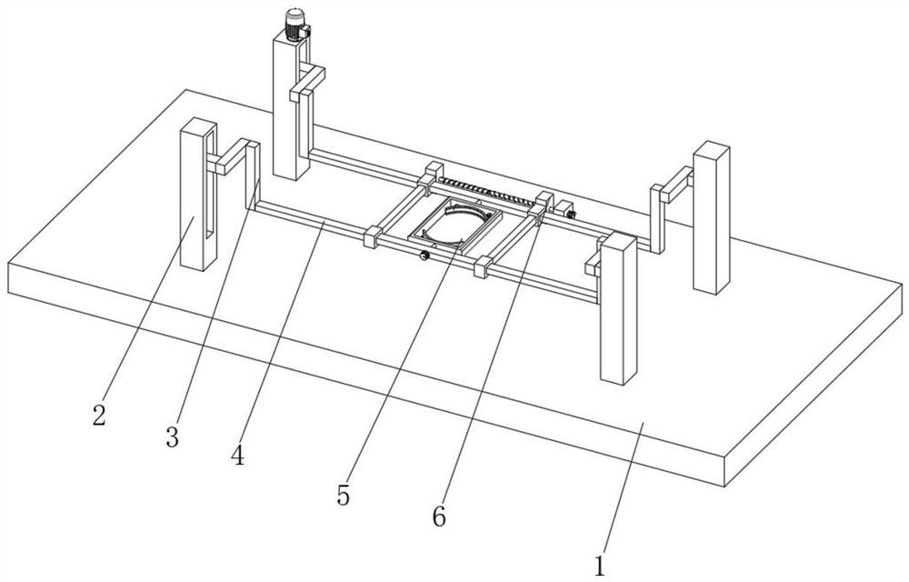
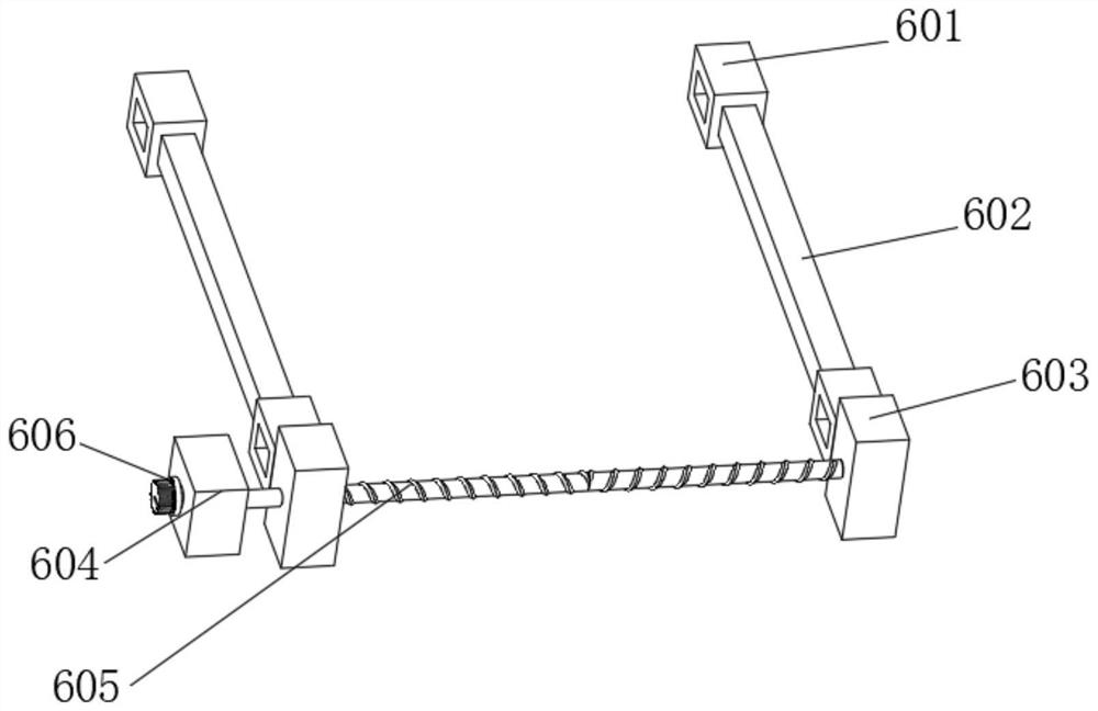
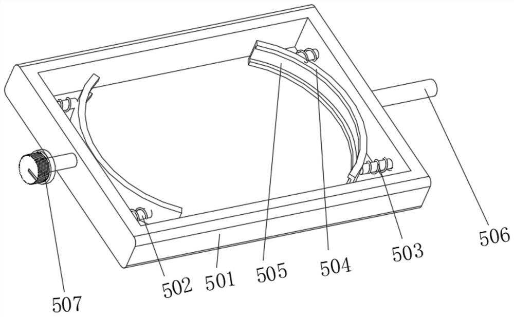
Electroplating clamp for compound semiconductor microwave chip
A microwave chip and electroplating fixture technology, applied in semiconductor devices, circuits, electrolysis processes, etc., can solve problems such as concentration of power lines, differences in metal ion concentration, defects in holes, etc. Effect
- Summary
- Abstract
- Description
- Claims
- Application Information
AI Technical Summary
Problems solved by technology
Method used
Image

Examples
Embodiment Construction
[0018] Next, the technical solutions in the embodiments of the present invention will be described in connection with the drawings of the embodiments of the present invention, and it is understood that the described embodiments are merely the embodiments of the present invention, not all of the embodiments. Based on the embodiments of the present invention, all other embodiments obtained by those of ordinary skill in the art are in the range of the present invention without making creative labor premise.
[0019] It should be noted that in the description of the present invention, the terms "top", "lower", "front", "post", "left", "right", "vertical", "horizontal", "top", The orientation or positional relationship of "bottom", "inside", "outside", etc. is based on the orientation or positional relationship shown in the drawings, is merely intended to describe the present invention and simplified description, is not indicated or implied. Or the component must have a specific orient...
PUM
 Abstract
Description
Claims
Application Information
 - R&D Engineer
- R&D Manager
- IP Professional
- Industry Leading Data Capabilities
- Powerful AI technology
- Patent DNA Extraction
Browse by: Latest US Patents, China's latest patents, Technical Efficacy Thesaurus, Application Domain, Technology Topic, Popular Technical Reports.
© 2024 PatSnap. All rights reserved.Legal|Privacy policy|Modern Slavery Act Transparency Statement|Sitemap|About US| Contact US: help@patsnap.com