


Quick Research
Generate reliable direction feasibility study reports for your R&D in just a few steps.

Technical Q&A
Discover and master advanced knowledge NOW. Basics, ideas, possibilities, all at once.

Find Solutions
As an expert in R&D theories, this can generate solutions to your technical problems instantly.

Evaluate Feasibility
Analyze your overall solution with one click, know your potential R&D risks in advance.

Monitor Landscape
Get weekly tech updates, stay abreast of the latest tech innovations and key insights.
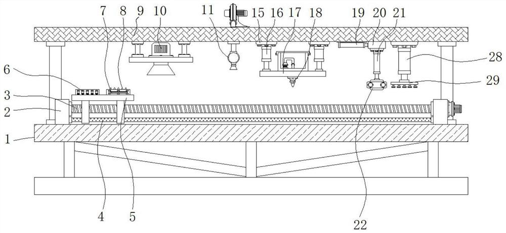
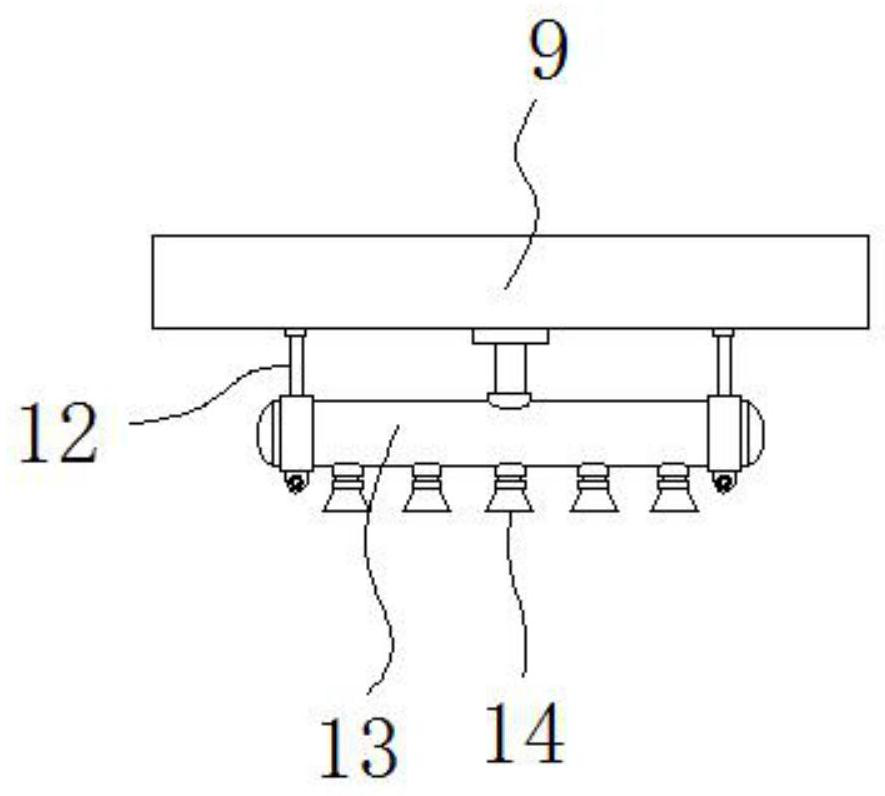
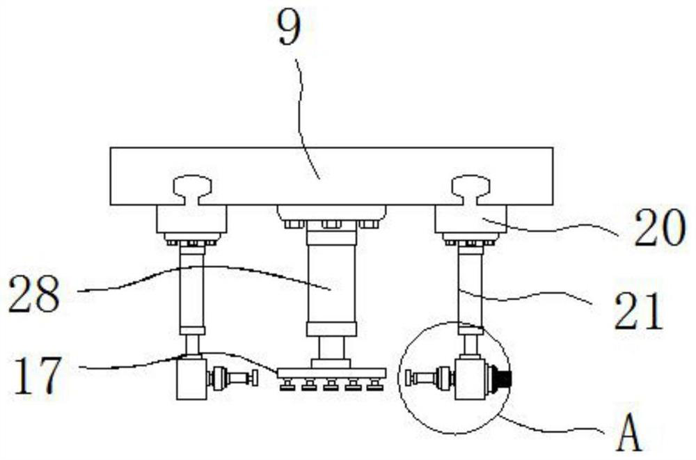
PCB and laminating process thereof
A PCB board and process technology, applied in the field of PCB board and its lamination process, can solve the problems of inconvenient dust removal of printed circuit boards, inconvenience of scanning and inspection of printed circuit boards, and inconvenience of extrusion and bonding of printed circuit boards, etc. The effect of improving stability and improving the pass rate
- Summary
- Abstract
- Description
- Claims
- Application Information
AI Technical Summary
Problems solved by technology
Method used
Image

Examples
Embodiment Construction
[0033] The following will clearly and completely describe the technical solutions in the embodiments of the present invention with reference to the accompanying drawings in the embodiments of the present invention. Obviously, the described embodiments are only some, not all, embodiments of the present invention.
[0034] In the description of the present invention, unless otherwise stated, the meaning of "plurality" is two or more; the terms "upper", "lower", "left", "right", "inner", "outer" , "front end", "rear end", "head", "tail", etc. indicate the orientation or positional relationship based on the orientation or positional relationship shown in the drawings, and are only for the convenience of describing the present invention and simplifying the description, rather than Nothing indicating or implying that a referenced device or element must have a particular orientation, be constructed, and operate in a particular orientation should therefore not be construed as limiting ...
PUM
 Abstract
Description
Claims
Application Information
 - R&D Engineer
- R&D Manager
- IP Professional
- Industry Leading Data Capabilities
- Powerful AI technology
- Patent DNA Extraction
Browse by: Latest US Patents, China's latest patents, Technical Efficacy Thesaurus, Application Domain, Technology Topic, Popular Technical Reports.
© 2024 PatSnap. All rights reserved.Legal|Privacy policy|Modern Slavery Act Transparency Statement|Sitemap|About US| Contact US: help@patsnap.com