Heterojunction cell and preparation method thereof, and solar cell module
A technology of a heterojunction cell and a transparent conductive layer is applied in the field of solar cells, which can solve the problems of weakening the electric field of the PN junction, increasing the recombination of photogenerated carriers, and low cell efficiency, so as to enhance the electric field strength, enhance the separation effect, and improve the efficiency. Effect
- Summary
- Abstract
- Description
- Claims
- Application Information
AI Technical Summary
Problems solved by technology
Method used
Image


Examples
Embodiment 1
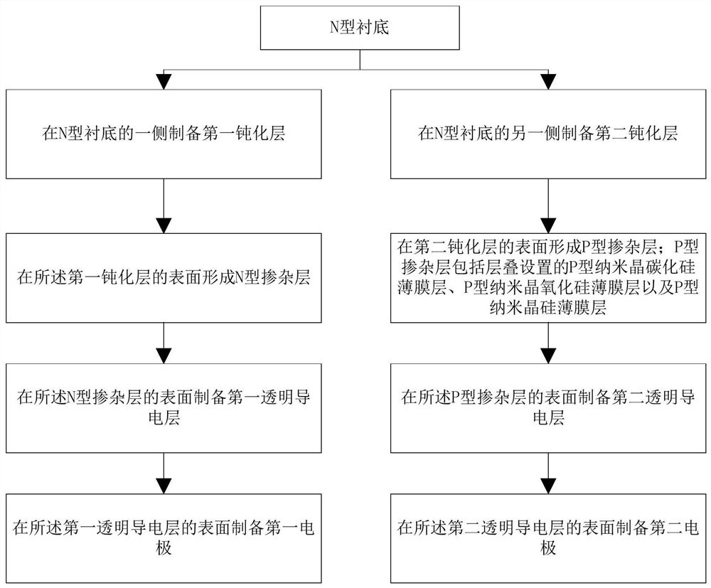
[0037] figure 1 It is a flowchart of the preparation method of the heterojunction battery in Example 1 of the present invention, such as figure 1 As shown, this embodiment provides a method for preparing a heterojunction battery, including the following steps: preparing a first passivation layer on one side (front side) of an N-type substrate, and preparing a second passivation layer on the other side (back side). A passivation layer; an N-type doped layer is formed on the surface of the first passivation layer, and a P-type doped layer is formed on the surface of the second passivation layer; the P-type doped layer includes a P-type nanocrystalline silicon film layer, also including a P-type nanocrystalline silicon oxide thin film layer and a P-type nanocrystalline silicon carbide thin film layer, and the P-type nanocrystalline silicon thin film layer and the P-type nanocrystalline silicon oxide thin film layer and the P-type nanocrystalline carbonized The silicon thin film ...
Embodiment 2
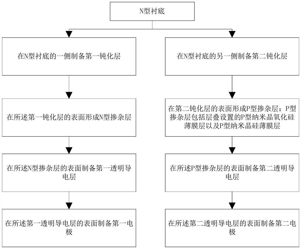
[0057] figure 2 It is a flow chart of the preparation method of the heterojunction battery in Example 2 of the present invention, Image 6 It is a schematic structural diagram of the heterojunction battery in Example 2 of the present invention. Such as figure 2 and Image 6 As shown, the difference between this embodiment and embodiment 1 is:
[0058] On the surface of the second passivation layer, the P-type doped layer is sequentially composed of a P-type nanocrystalline silicon oxide thin film layer and a P-type nanocrystalline silicon thin film layer. When forming the P-type doped layer, a P-type nanocrystalline silicon oxide thin film layer is first formed on the second passivation layer, and then a P-type nanocrystalline silicon oxide thin film layer is formed on the P-type nanocrystalline silicon oxide thin film layer.
[0059] For other layer structures and preparation processes, reference may be made to the corresponding layer structures and preparation processe...
Embodiment 3
[0061] image 3 It is a flowchart of the preparation method of the heterojunction battery in Example 3 of the present invention, Figure 7 It is a schematic structural diagram of the heterojunction battery in Example 3 of the present invention. Such as image 3 and Figure 7 Shown, the difference between this embodiment and embodiment 1, embodiment 2 is:
[0062] The P-type doped layer on the surface of the second passivation layer is sequentially composed of a P-type nanocrystalline silicon carbide thin film layer and a P-type nanocrystalline silicon thin film layer from inside to outside. When forming the P-type doped layer, a P-type nanocrystalline silicon carbide thin film layer is first formed on the second passivation layer, and then a P-type nanocrystalline silicon carbide thin film layer is formed on the P-type nanocrystalline silicon carbide thin film layer.
[0063] For other layer structures and preparation processes, reference may be made to the corresponding l...
PUM
| Property | Measurement | Unit |
|---|---|---|
| Thickness | aaaaa | aaaaa |
| Thickness | aaaaa | aaaaa |
| Thickness | aaaaa | aaaaa |
Abstract
Description
Claims
Application Information
 - R&D
- Intellectual Property
- Life Sciences
- Materials
- Tech Scout
- Unparalleled Data Quality
- Higher Quality Content
- 60% Fewer Hallucinations
Browse by: Latest US Patents, China's latest patents, Technical Efficacy Thesaurus, Application Domain, Technology Topic, Popular Technical Reports.
© 2025 PatSnap. All rights reserved.Legal|Privacy policy|Modern Slavery Act Transparency Statement|Sitemap|About US| Contact US: help@patsnap.com