
Transfer printing forming method for metallized circuit of plastic part

A molding method and metallization technology, which is applied to the printing of special varieties of printed matter, copying/marking methods, ink transfer from original manuscripts, etc., can solve the problems of difficult to make a high-gloss surface, long laser laser process, and product surface discoloration, etc. problems, to achieve high reliability test requirements, fast processing efficiency, and low cost effects

Inactive Publication Date: 2021-10-08
KUNSHAN LIANTAO ELECTRONICS CO LTD
View PDF8 Cites 0 Cited by
  • Summary
  • Abstract
  • Description
  • Claims
  • Application Information

AI Technical Summary

Problems solved by technology

[0006] The traditional LDS (Laser Direct Structuring) process requires special plastic materials and special laser equipment. The laser laser process is long, requires copper plating, nickel plating and then gold plating, and the cost of electroless plating is extremely high, and modified PC, PA, PC are used +The toughness of ABS material is not as good as that of ordinary materials, and the surface of the product will change color after chemical plating, and it is not easy to make a high-gloss surface. Therefore, we have improved this and proposed a transfer molding method for metallized lines of plastic parts.

Method used


Image

  • Transfer printing forming method for metallized circuit of plastic part
  • Transfer printing forming method for metallized circuit of plastic part

Examples


Embodiment

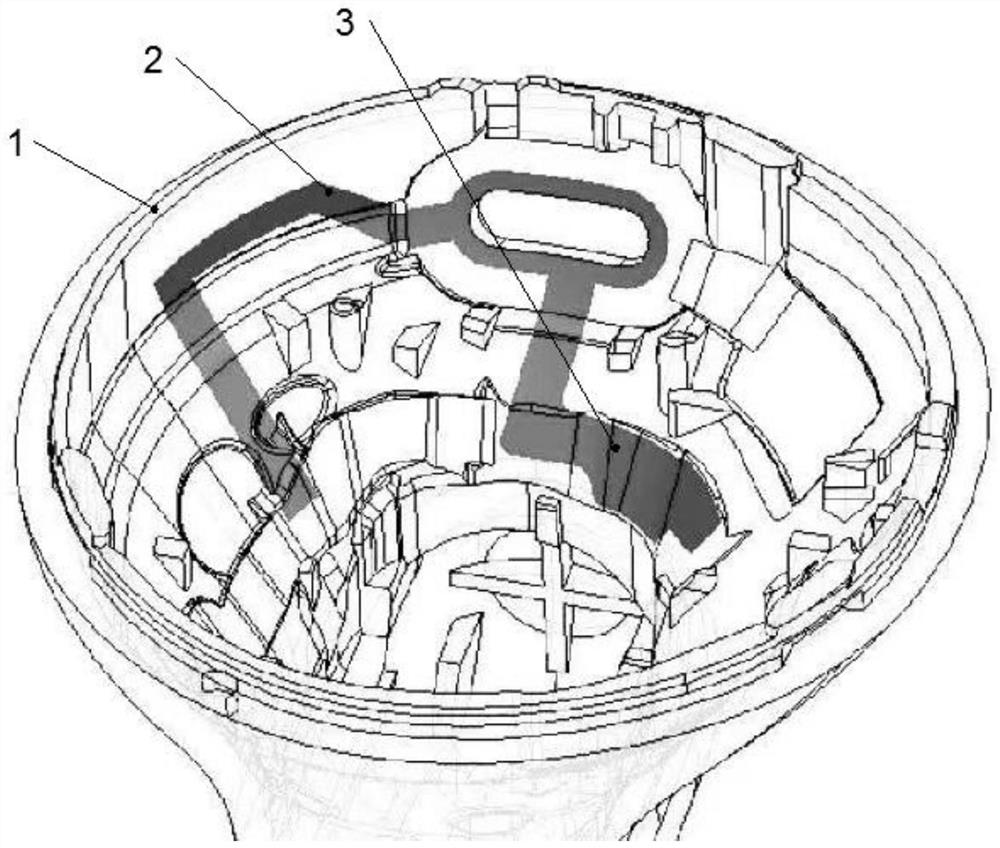
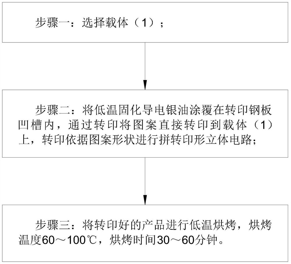
[0023] Example: such as Figure 1-2 As shown, the present invention is a transfer molding method for metallized circuits of plastic parts, comprising the following steps:

[0024] Step 1: Select carrier 1;

[0025] Step 2: Coat the low-temperature curing conductive silver oil in the groove of the transfer printing steel plate, transfer the pattern directly to the carrier 1 by transfer printing, and transfer the three-dimensional circuit according to the shape of the pattern;

[0026] Step 3: Baking the transferred product at a low temperature at a temperature of 60-100° C. and a baking time of 30-60 minutes.

[0027] Wherein, the carrier is plastic.

[0028] Wherein, the carrier is glass.

[0029] Wherein, the conductive silver oil in step 2 is polyester system conductive silver oil, and the thickness of the conductive silver oil is 0.09-0.16mm.

[0030] Among them, in step 2, the transfer printing includes antenna printing 2 and power feeding printing 3, and there is no s...


PUM

PropertyMeasurementUnit
Thicknessaaaaaaaaaa

Abstract

The invention discloses a transfer printing forming method for a metallized circuit of a plastic part. The transfer printing forming method comprises the following steps: step 1, a carrier is selected; 2, low-temperature curing conductive silver oil is coated in a transfer printing steel plate groove, a pattern is directly transferred to the carrier through transfer printing, and transfer printing is carried out according to the pattern shape to form a three-dimensional circuit; and 3, the transferred product is subjected to low-temperature baking, the baking temperature ranges from 60 DEG C to 100 DEG C, and the baking time ranges from 30 min to 60 min. The transfer printing forming method for the metallized circuit of the plastic part has no special requirements on a plastic carrier material, a PPS process can coat conductive silver oil on a plastic carrier through a transfer printing (gravure printing) technology, a 3D circuit can be realized through a transfer printing splicing process, a conductive circuit can be quickly formed, the PPS process can be suitable for material carriers such as PPA, PC, ABS, PC + ABS, PPA, PET, PI and glass. The PPS process can directly transfer required circuit patterns on the surface and the inner side of the carrier, and a circuit is formed through low-temperature baking.

Description

technical field [0001] The invention relates to the technical field of circuit transfer printing, in particular to a transfer printing forming method for metalized circuits of plastic parts. Background technique [0002] Extruded plastic surface thermal transfer metal film decoration products apply the thermal transfer film printing process to the plastic extrusion product process, using dot printing (resolution 300dpi) to paint metal, stainless steel wire drawing, wood grain, marble, etc. The pattern is printed on the surface of PET and polyester film, and then transferred to the surface of the plastic extruded product by thermal transfer printing. After the product is formed, the transfer layer and the plastic surface are integrated with high metal texture (or wood grain, marble grain, etc.) Decorative products, this process can decorate the surface, side and end surface of extruded products, can decorate arc, 3600, special-shaped surface, serrated surface, and seamless co...

Claims


Application Information

Patent Timeline
IPC IPC(8): B41M3/06B41M5/00B41M5/025B41M7/00
CPCB41M3/06B41M5/025B41M5/0064B41M5/007B41M7/009
Inventor 张云青张文亮王东方王立平
Owner KUNSHAN LIANTAO ELECTRONICS CO LTD
Learn More