
Semiconductor wafer protection film tearing structure and operation method

A semiconductor and film structure technology, applied in the field of semiconductor wafer protection tear film structure, can solve the problems of inability to tear the film, surface rubbing of semiconductor wafers, low height, etc. block effect

Active Publication Date: 2021-10-08
JIANGSU NEPES SEMICON
View PDF4 Cites 2 Cited by
  • Summary
  • Abstract
  • Description
  • Claims
  • Application Information

AI Technical Summary

Problems solved by technology

[0006] The object of the present invention is to provide a semiconductor wafer protection tear film structure and operation method, to solve the existing semiconductor wafer tear film equipment proposed in the above-mentioned background technology , In the process of tearing the film, there are very high precision requirements for the height of the reverse-rotating guide roller. If the reverse-rotating guide roller is too high, the protective film cannot be torn off. The surface of the wafer is scratched, which has great disadvantages, so that a batch of defective semiconductor wafers will appear during the film tearing process, and the protective film torn by the reverse guide roller is easy to stick to the surface of the reverse guide roller. During the process of rubbing and tearing the film by the roller against the next semiconductor wafer, the surface of the protective film is smooth, resulting in the situation that the film cannot be torn off, and manual cleaning is required

Method used


Image

  • Semiconductor wafer protection film tearing structure and operation method
  • Semiconductor wafer protection film tearing structure and operation method
  • Semiconductor wafer protection film tearing structure and operation method

Examples


Embodiment 1

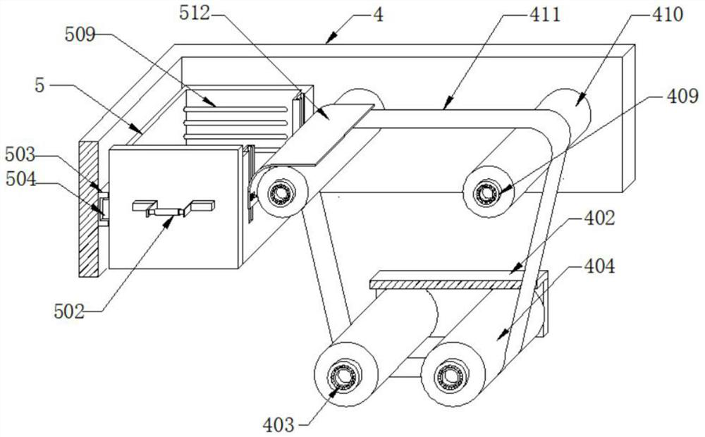
[0039] A number of hydraulic rods 401 are fixed on the top of the inner cavity of the tearing film chamber 4, and the output ends of the hydraulic rods 401 are located below. The output ends of the hydraulic rods 401 are fixed with a mounting frame 402, and the front and rear ends of the mounting frame 402 are fitted with several first bearings respectively. 403, a pressure roller 404 is fixed between the two rotating ends of the first bearing 403, at least two pressure rollers 404 are provided, a driving motor 405 is fixed on one side of the upper end surface of the mounting frame 402, and the output end of the driving motor 405 is fixed with The driving wheel 406 and one end of the pressure roller 404 run through the first bearing 403 and are fixedly connected to the rotating end with a driven plate 407, and a transmission belt 408 is sleeved between the driven plate 407 and the driving wheel 406, and the two ends of the inner cavity of the tear film chamber 4 are respectively...

Embodiment 2

[0041] see Figure 2-7 , and the difference from Embodiment 1 is that an open end 501 is provided on one side of the front end of the tearing film bin 4, and the collecting bin 5 is movably socketed with the opening end 501, and a handle 502 is fixed on the front end of the collecting bin 5, and the tearing film One side of the inner chamber of bin 4 is fixed with a chute 503 arranged in parallel, and the inner cavity of the chute 503 is socketed with a slider 504, which is fixedly connected with one side of the collection bin 5, and the middle end of the inner cavity of the collection bin 5 A partition 505 is fixed to divide the collection bin 5 into two chambers. A plurality of through holes 506 are equidistantly provided in the partition 505, and a passage 507 is provided at the center line of the partition 505, and the passage 507 is locked. A plug body 508 is connected, and a plurality of heating tubes 509 are respectively arranged on both sides of the inner chamber of th...

Embodiment 3

[0043] see Figure 4-7 The difference from Embodiment 1 is that: one end surface of the collection bin 5 close to the rotating roller 410 is provided with a plurality of locking grooves 510, and the inner cavity of the plurality of locking grooves 510 is sleeved with a locking block 511, and the locking block 511 is close to the rotating roller 410 A shovel plate 512 is fixed on the surface of one end of the shovel plate 512 and a bolt 513 is threaded inside the block 511, and one end of the bolt 513 is movably connected with the slot 510, and the shovel plate 512 can move up and down in the slot 510 through the block 511, thereby Make shoveling plate 512 can fit on the surface of adhesive tape 411, carry out shoveling operation to its surface, shoveling plate 512 upper end side arcs downwards, the protective film or viscose that can be shoveled can be sent in the collection bin 5.

[0044] It is worth noting that: the driving motor 405 in this technical solution adopts a gear...


PUM


Abstract

The invention discloses a semiconductor wafer protection film tearing structure which comprises a workbench and a film tearing bin arranged above the workbench and used for sticking and tearing a semiconductor wafer protection film. According to the device, two pressing rollers rotate in the same direction and are used for extruding and assisting a semiconductor wafer on a strip-shaped conveying belt to move, an adhesive tape connected with the surfaces of the pressing rollers and rotating rollers in a sleeving mode can bond an extruded semiconductor wafer protection film, the adhesive tape and the pressing rollers rotate in the same direction, but the semiconductor wafer protection film bonded with the adhesive tape can be bonded by the adhesive tape to move upwards, the two pressing rollers enable the semiconductor wafer to be transversely arranged on the strip-shaped conveying belt, so that the semiconductor wafer protection film is pulled and the semiconductor wafer is uncovered, the processing efficiency is high, and continuous film tearing operation can be conducted on the semiconductor wafer; and the height of the pressing rollers is adjusted in advance through driving of a hydraulic rod, height adjustment does not need to be conducted in the later period, the situation that the semiconductor wafer is extruded and damaged due to adjustment errors caused by frequent adjustment of the pressing rollers is prevented.

Description

technical field [0001] The invention relates to the technical field of semiconductor tearing film equipment, in particular to a semiconductor wafer protection tearing film structure and an operation method. Background technique [0002] Wafer refers to the silicon wafer used to make silicon semiconductor integrated circuits. Its raw material is silicon. High-purity polysilicon is dissolved and mixed with silicon crystal seeds, and then slowly pulled out to form cylindrical single crystal silicon, silicon crystal After the rod is ground, polished, and sliced, it forms a silicon wafer, that is, a wafer. During the storage process of the semiconductor wafer, a layer of PET transparent material protective film needs to be covered on the surface to prevent the surface of the semiconductor wafer from appearing. Friction and scratching, before processing the semiconductor wafer, the surface protective film needs to be peeled off. [0003] The normal working process is: put the sem...

Claims


Application Information

Patent Timeline
IPC IPC(8): B32B43/00
CPCB32B43/006
Inventor 张乔栋程凯袁泉
Owner JIANGSU NEPES SEMICON
Learn More