Method for manufacturing PCB crimping hole

A technology of crimping holes and PCB boards, which is applied in the direction of printed circuit manufacturing, electrical connection of printed components, and formation of electrical connections of printed components. and other issues to achieve the effect of improving signal transmission efficiency and reducing signal transmission loss

Pending Publication Date: 2021-09-17
广州广合科技股份有限公司
View PDF6 Cites 0 Cited by
  • Summary
  • Abstract
  • Description
  • Claims
  • Application Information

AI Technical Summary

Problems solved by technology

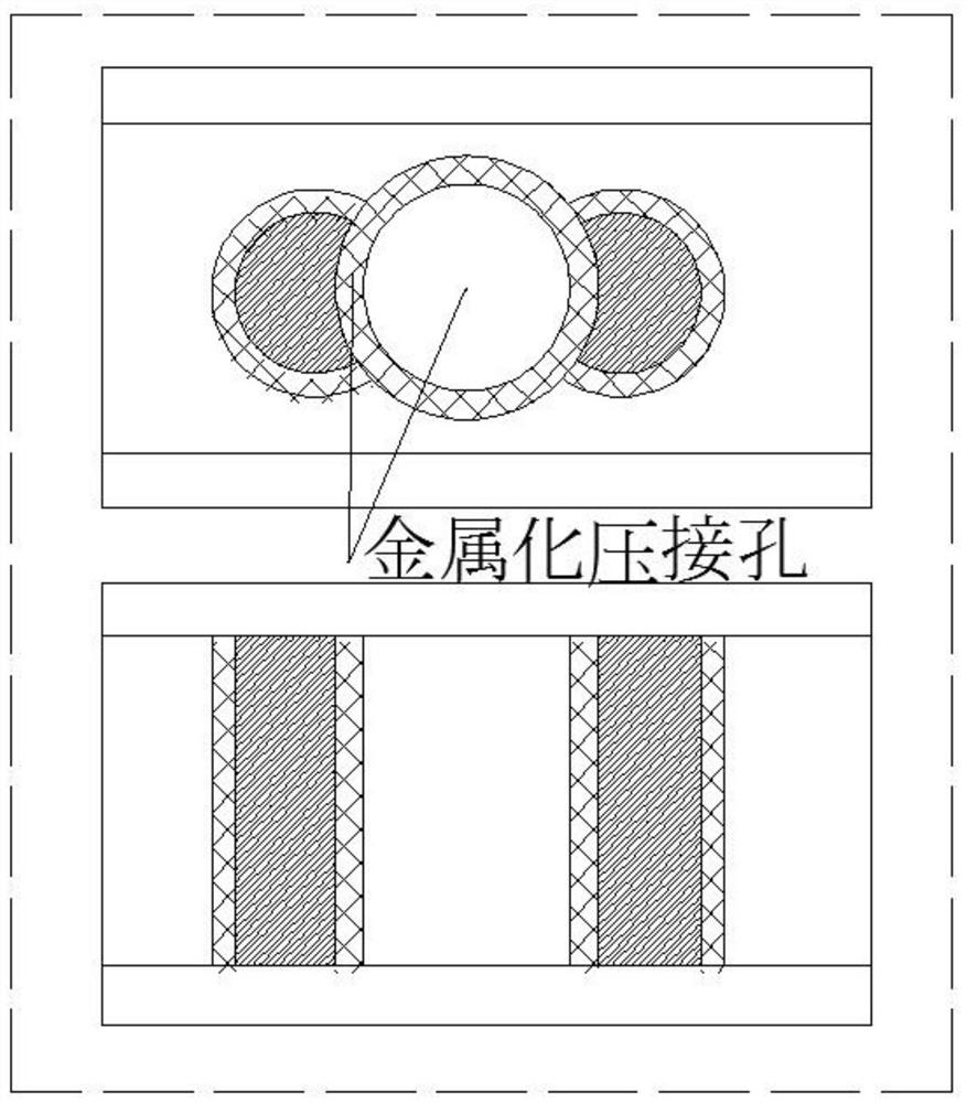
In the actual production of PCB crimping holes, the design of the crimping hole is generally a single hole. The design structure of the single hole is relatively simple, without signal shielding function, and gradually cannot meet the requirements of high-speed transmission of signals in the crimping hole, and cannot achieve the effect required by customers.

Method used


Image

  • Method for manufacturing PCB crimping hole
  • Method for manufacturing PCB crimping hole
  • Method for manufacturing PCB crimping hole

Examples


Embodiment Construction

[0022] Preferred embodiments of the present application will be described in more detail below with reference to the accompanying drawings. Although preferred embodiments of the present application are shown in the drawings, it should be understood that the present application may be embodied in various forms and should not be limited to the embodiments set forth herein. Rather, these embodiments are provided so that this application will be thorough and complete, and will fully convey the scope of this application to those skilled in the art.

[0023] The terminology used in this application is for the purpose of describing particular embodiments only, and is not intended to limit the application. As used in this application and the appended claims, the singular forms "a", "the", and "the" are intended to include the plural forms as well, unless the context clearly dictates otherwise. It should also be understood that the term "and / or" as used herein refers to and includes a...


PUM


Abstract

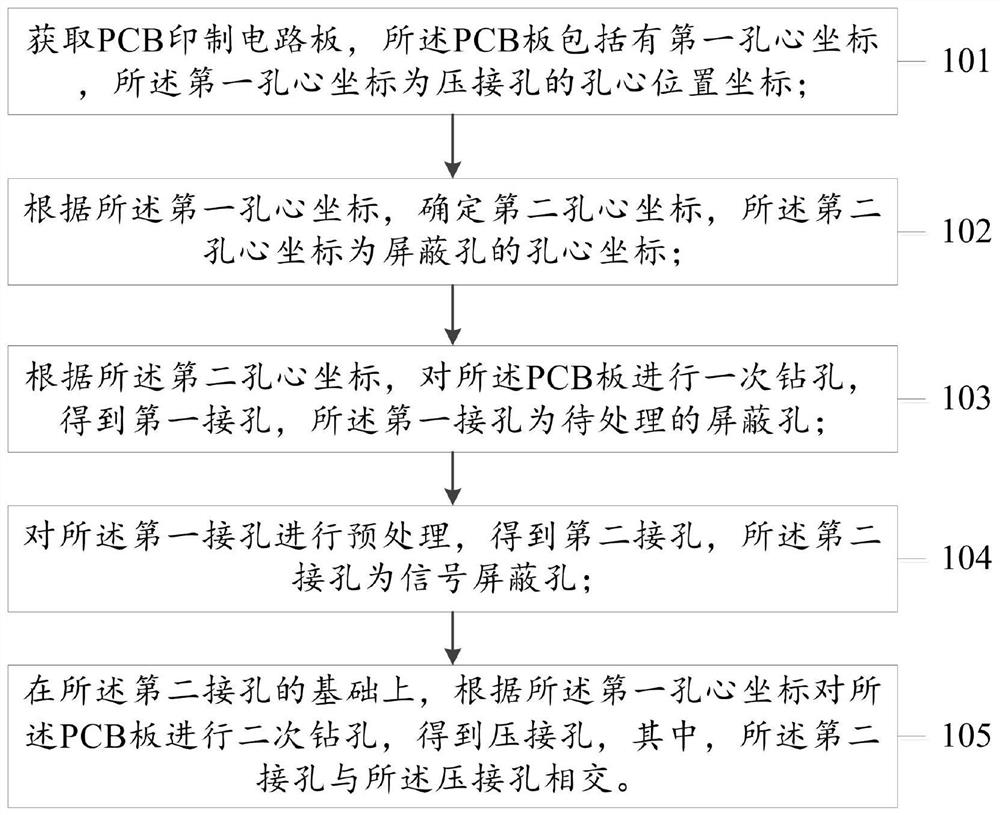
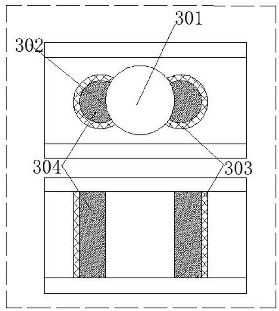
The invention relates to a method for manufacturing a PCB crimping hole. The method comprises the steps: acquiring a PCB, wherein the PCB comprises a first hole center coordinate, and the first hole center coordinate is a hole center position coordinate of a crimping hole; according to the first hole center coordinate, determining a second hole center coordinate, wherein the second hole center coordinate is the hole center coordinate of the shielding hole; according to the second hole center coordinate, carrying out the drilling on the PCB for the first time to obtain a first connecting hole, wherein the first connecting hole is a shielding hole to be processed; preprocessing the first connecting hole to obtain a second connecting hole, wherein the second connecting hole is a signal shielding hole; on the basis of the second connecting hole, carrying out the secondary drilling on the PCB according to the first hole center coordinate, and obtaining a crimping hole, wherein the second connecting hole intersects with the crimping hole. According to the scheme provided by the invention, the shielding hole has a signal shielding function, so that the signal transmission loss of the crimping hole is reduced, and the signal transmission efficiency of the crimping hole is improved.

Description

technical field [0001] The present application relates to the technical field of making crimping holes, in particular to a method for making PCB crimping holes. Background technique [0002] PCB printed circuit board (printed circuit board) is one of the important components of the electronics industry. Almost every electronic device, ranging from electronic watches and calculators to computers, communication electronic equipment, and military weapon systems, must use printed circuit boards. Board; With the development of various technical equipment, the quality requirements for printed circuit boards are getting higher and higher, especially for the signal transmission quality of PCB lines. [0003] The crimping hole is a special through hole on the PCB. It does not require soldering. It is a hole that can be fixed by inserting components directly. The crimping hole conducts current through the contact between the pin and the hole wall, thereby realizing signal transmission...

Claims


Application Information

Patent Timeline
Patent Type & Authority Applications(China)
IPC IPC(8): H05K1/02H05K1/11H05K3/42
CPCH05K1/0222H05K1/115H05K3/423H05K3/425H05K2201/095
Inventor 兰富民胡伦洪田玲钟根带叶圣涛
Owner 广州广合科技股份有限公司
Why Eureka
Try Eureka