Photoelectrochemical optical fiber microelectrode adopting electrode internal illumination mode and preparation method of photoelectrochemical optical fiber microelectrode
A photoelectrochemical and microelectrode technology, applied in the fields of photoelectrochemistry and analytical chemistry, can solve the problems of large size and limited wavelength of light source, and achieve the effect of simple operation and significant photoelectric signal
- Summary
- Abstract
- Description
- Claims
- Application Information
AI Technical Summary
Problems solved by technology
Method used
Image
Examples
Embodiment 1
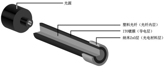
[0040] Polishing of optical fiber:
[0041] Commercially available plastic optical fiber with a diameter of 1.0 mm, transparent and colorless, the core material is modified polymethylmethacrylate (PMMA), the cladding material is oxygen resin, the minimum bending radius is 10 times the fiber diameter, and the length of white light transmission 25~30 m, the fiber specification tolerance is 6% of the diameter. Cut the optical fiber into small sections of 9-10 cm, and use sandpaper to polish one end of the small optical fiber section at 360 degrees to obtain a frosted surface with a length of about 1.0 cm. Finally, the polished optical fiber was ultrasonically cleaned with ethanol and ultrapure water in sequence.
[0042] Preparation of optical fiber conductive film:
[0043] A conductive film is plated on the polished optical fiber by DC sputtering. The conductive film material is indium tin oxide (ITO), and the coating adopts the JCP-350M3 coating machine of Beijing Techno Te...
Embodiment 2
[0051] The steps of polishing the optical fiber and preparing the conductive film of the optical fiber are the same as those in Example 1.
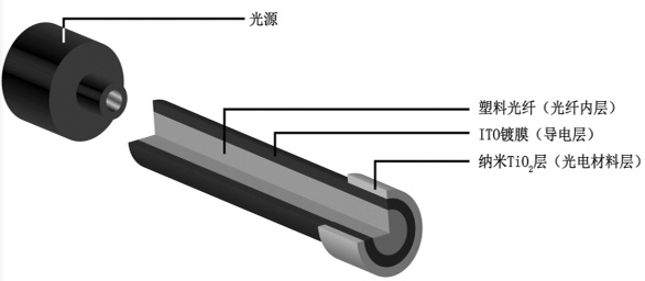
[0052] Preparation of optical fiber photoelectric material layer: In this case, titanium dioxide (TiO 2 ) as an example of optoelectronic materials. Preparation by dipping method: disperse the pre-prepared semiconductor nanoparticles with a solvent. Commercially available TiO with a particle size of about 20 nm was selected 2 Nanoparticles are used as photoelectric materials, and a dispersion solution with a concentration of 1.0 mg / mL is prepared with ultrapure water, and the dispersion solution is dipped in the frosted end of an optical fiber and dried at 37 °C. This process was repeated 3 times. That is, TiO is loaded on the conductive fiber 2 nano layer.
[0053] TiO in case 2 It can be replaced with other semiconductor materials, and the corresponding experimental parameters can be changed accordingly. A fiber optic electrode w...
PUM
| Property | Measurement | Unit |
|---|---|---|
| Diameter | aaaaa | aaaaa |
| Particle size | aaaaa | aaaaa |
| Particle size | aaaaa | aaaaa |
Abstract
Description
Claims
Application Information
 - R&D
- Intellectual Property
- Life Sciences
- Materials
- Tech Scout
- Unparalleled Data Quality
- Higher Quality Content
- 60% Fewer Hallucinations
Browse by: Latest US Patents, China's latest patents, Technical Efficacy Thesaurus, Application Domain, Technology Topic, Popular Technical Reports.
© 2025 PatSnap. All rights reserved.Legal|Privacy policy|Modern Slavery Act Transparency Statement|Sitemap|About US| Contact US: help@patsnap.com


