Chip unit and chip assembly

A chip unit and chip technology, which is applied in the field of chip units and chip components, can solve problems such as easy cracking of bumps, chip failure, and unstable connection between chips and packaging structures, so as to reduce the probability of cracking, ensure stability, and increase The effect of setting the density

Pending Publication Date: 2021-08-27
XI AN UNIIC SEMICON CO LTD
View PDF0 Cites 1 Cited by
  • Summary
  • Abstract
  • Description
  • Claims
  • Application Information

AI Technical Summary

Problems solved by technology

[0002] In the field of semiconductor technology, bumps are usually formed on the chip, and the bumps are connected to the metal layer inside the chip. During the chip packaging process, wires need to be bonded on the bumps, and then the wires are connected to the packaging structure to realize chip signals. transmission, but in the current technology only according to the structural design of the chip, bumps for bonding wires are set on some areas of the chip, and these bumps are prone to cracks due to uneven stress during manufacturing or use , causing the connection between the chip and the package structure to be unstable, causing the chip to fail

Method used


Image

  • Chip unit and chip assembly
  • Chip unit and chip assembly
  • Chip unit and chip assembly

Examples


Embodiment Construction

[0033] In order to understand the above-mentioned purpose, features and advantages of the present invention more clearly, the present invention will be further described in detail below in conjunction with the accompanying drawings and specific embodiments. It should be noted that, in the case of no conflict, the embodiments of the present application and the features in the embodiments can be combined with each other.

[0034] In the following description, many specific details are set forth in order to fully understand the present invention. However, the present invention can also be implemented in other ways different from those described here. Therefore, the protection scope of the present invention is not limited by the specific details disclosed below. EXAMPLE LIMITATIONS.

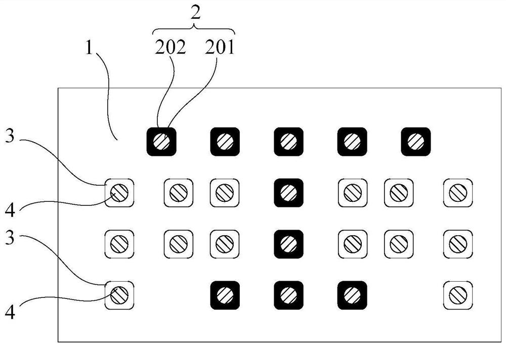
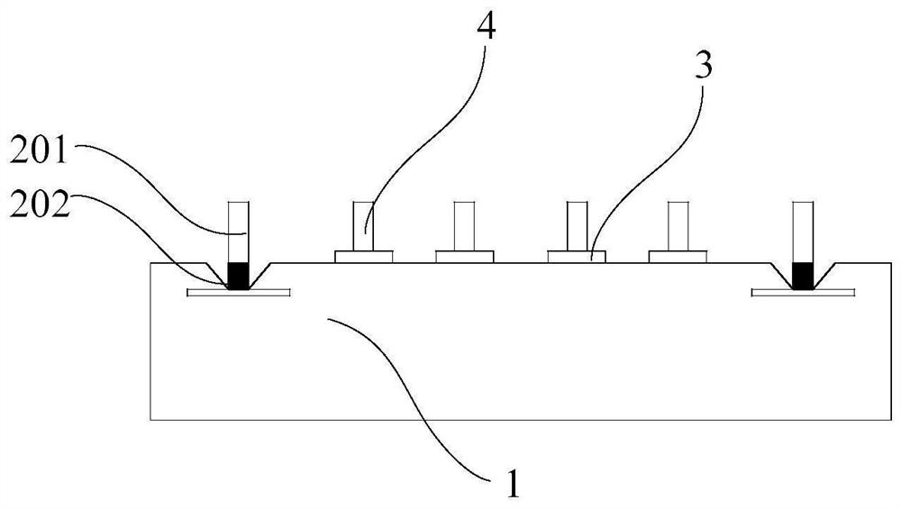
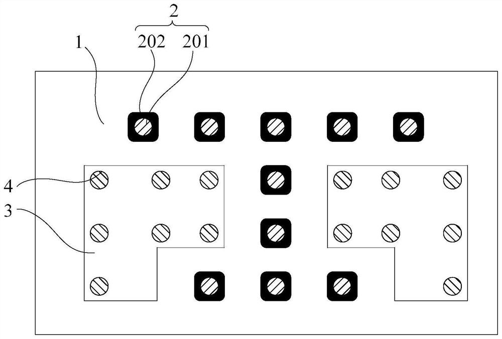
[0035] Such as Figure 1 to Figure 5 As shown, according to the first aspect of the embodiment of the present application, a chip unit is proposed including: a substrate 1; a conductive component 2 ...


PUM


Abstract

The invention provides a chip unit and a chip assembly, and the chip unit comprises a substrate; a conductive assembly and redundant salient points; the conductive assembly is arranged on a partial area of the substrate, the conductive assembly comprises a first salient point and a first bonding pad, the first bonding pad is arranged on the substrate, and the first salient point is arranged on the first bonding pad; and the redundant salient points are arranged on the other part of the area of the substrate. According to the chip unit, the cracking probability of the first salient points can be reduced, and the stability of connection between the chip unit and the packaging structure can be guaranteed; and the stress distribution on the substrate can be more uniform, so that the function of protecting functional modules in the chip unit can be achieved, and the probability of functional failure of the chip unit can be reduced.

Description

technical field [0001] The present invention relates to the technical field of semiconductors, in particular to a chip unit and a chip component. Background technique [0002] In the field of semiconductor technology, bumps are usually formed on the chip, and the bumps are connected to the metal layer inside the chip. During the chip packaging process, wires need to be bonded on the bumps, and then the wires are connected to the packaging structure to realize chip signals. transmission, but in the current technology only according to the structural design of the chip, bumps for bonding wires are set on some areas of the chip, and these bumps are prone to cracks due to uneven stress during manufacturing or use , resulting in an unstable connection between the chip and the package structure, causing chip failure. Contents of the invention [0003] The present invention aims to solve at least one of the technical problems existing in the prior art or related art. [0004] I...

Claims


Application Information

Patent Timeline
Patent Type & Authority Applications(China)
IPC IPC(8): H01L23/488
CPCH01L23/488H01L24/14H01L2224/1412H01L2224/14515
Inventor 韩彦武包谦
Owner XI AN UNIIC SEMICON CO LTD
Why Eureka
Try Eureka