Printed circuit board (PCB) printing and copper plating equipment and technology

A PCB board and copper plating technology, which is applied in the direction of printed circuit, printed circuit manufacturing, and electrical connection formation of printed components, etc., can solve problems such as poor cleaning effect, uneven electroplating coating, and insufficient precision of copper plating, etc., and achieve better results , Efficiency and average thickness, the effect of uniform coating thickness

Active Publication Date: 2021-08-24
中山家普乐电子科技有限公司
View PDF7 Cites 0 Cited by
  • Summary
  • Abstract
  • Description
  • Claims
  • Application Information

AI Technical Summary

Problems solved by technology

[0006] Aiming at the deficiencies of the prior art, the present invention provides a PCB board printing copper plating equipment, which has the advantages of being able to adapt to various PCB boards of different specifications, good cleaning effect, accurate copper plating, high copper plating efficiency, etc., and solves the problem of cleaning effect. Poor, uneven electroplating layer, copper plating is not accurate enough

Method used


Image

  • Printed circuit board (PCB) printing and copper plating equipment and technology
  • Printed circuit board (PCB) printing and copper plating equipment and technology
  • Printed circuit board (PCB) printing and copper plating equipment and technology

Examples


Embodiment Construction

[0041] The following will clearly and completely describe the technical solutions in the embodiments of the present invention with reference to the accompanying drawings in the embodiments of the present invention. Obviously, the described embodiments are only some, not all, embodiments of the present invention. Based on the embodiments of the present invention, all other embodiments obtained by persons of ordinary skill in the art without making creative efforts belong to the protection scope of the present invention.

[0042] As introduced in the background technology, there are deficiencies in the prior art. In order to solve the above technical problems, the present application proposes a printed copper plating equipment for PCB boards.

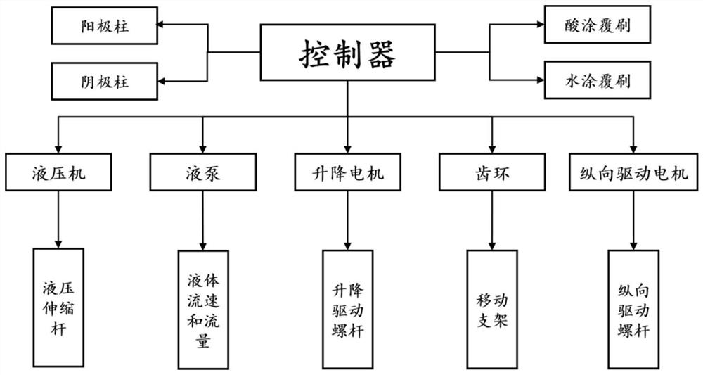
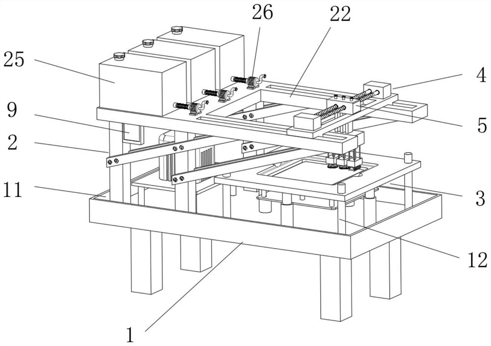
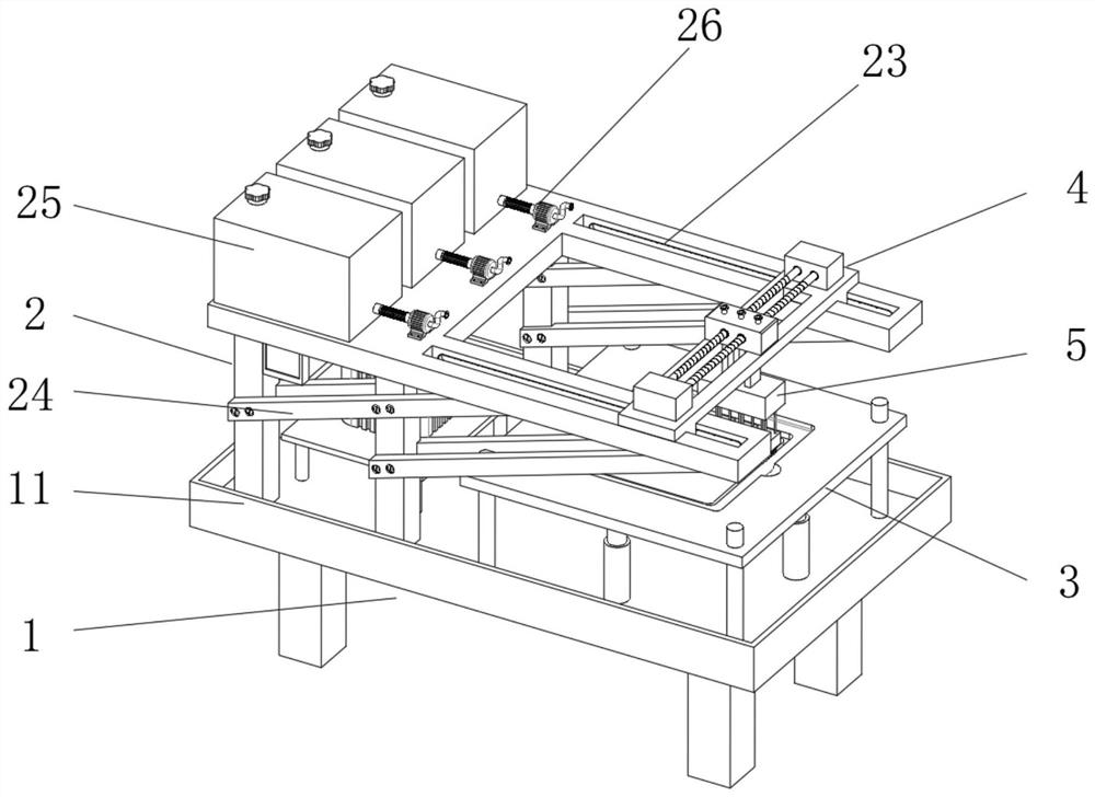
[0043] see Figure 1-12 , a PCB board printing copper plating equipment, including a support platform 1, a hydraulic press 14, a number of liquid storage tanks 25, a number of liquid pumps 26 and a controller 9, a support frame 2 is arran...


PUM


Abstract

The invention relates to the technical field of printed circuit board processing, and discloses PCB printing and copper plating equipment and a technology. The PCB printing and copper plating equipment comprises a supporting table, a supporting frame is arranged on one side of the top end of the supporting table, a supporting platform and two supporting cross beams are erected at the top end of the supporting frame, and a transverse moving mechanism is erected on the two supporting cross beams; and an operating mechanism is erected in the transverse moving mechanism and comprises a positioner at the top end, a connecting flow divider, a pickling device, a water scrubber and an electroplating device, wherein the pickling device, the water scrubber and the electroplating device are arranged on the lower surface of the connecting flow divider in a hanging manner. Under the control of a controller, the whole process can be orderly and rapidly carried out in a mode similar to printing, the electroplating effect is guaranteed, meanwhile, pickling, water washing and electroplating steps can be synchronously carried out, the time of full-plate pickling and water washing in the conventional steps is shortened, it is ensured that stain removal and electroplating processes of all point positions are effectively carried out, meanwhile, the time required by all procedures is effectively shortened, accordingly, the overall production efficiency is improved, and the copper plating capacity is increased.

Description

technical field [0001] The invention relates to the technical field of printed circuit board processing, in particular to a PCB printing copper plating equipment and a printing copper plating process. Background technique [0002] PCB circuit board, also known as printed circuit board, is the provider of electrical connection for electronic components. Its development has a history of more than 100 years. Its design is mainly layout design. The main advantage of using circuit boards is that it greatly reduces wiring and assembly errors and improves the automation level. In the PCB manufacturing process, many processes involve electroplating. The electroplating process plays a very important role in the PCB production process and affects the electrical conductivity of the PCB. [0003] The existing electroplating process is usually carried out in the electroplating tank. Before electroplating, the PCB board needs to be pickled and washed before electroplating. In this proces...

Claims


Application Information

Patent Timeline
Patent Type & Authority Applications(China)
IPC IPC(8): C25D19/00C25D17/00C25D3/38C25D7/00C25D5/00C25D5/06C25D5/02H05K3/42B08B1/04B08B3/08
CPCC25D17/00C25D3/38C25D7/00C25D5/00C25D5/06C25D5/02H05K3/424B08B1/002B08B1/005B08B1/04B08B3/08
Inventor 李柯胡家梦
Owner 中山家普乐电子科技有限公司
Why Eureka
Try Eureka