


Quick Research
Generate reliable direction feasibility study reports for your R&D in just a few steps.

Technical Q&A
Discover and master advanced knowledge NOW. Basics, ideas, possibilities, all at once.

Find Solutions
As an expert in R&D theories, this can generate solutions to your technical problems instantly.

Evaluate Feasibility
Analyze your overall solution with one click, know your potential R&D risks in advance.

Monitor Landscape
Get weekly tech updates, stay abreast of the latest tech innovations and key insights.
PLC chip, single-fiber bidirectional optical assembly, optical module and working method
A single-fiber bidirectional, optical component technology, applied in the field of optical communication, which can solve the problems of wavelength resource consumption, large wavelength interval, and fiber resource consumption.
- Summary
- Abstract
- Description
- Claims
- Application Information
AI Technical Summary
Problems solved by technology
Method used
Image

Examples
Embodiment 1
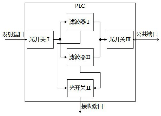
[0078] A kind of planar optical waveguide PLC chip, see figure 1 As shown, including transmitting port, filter element, receiving port and common port;
[0079] The transmitting port communicates with the filter element through an optical transmission channel I, and an optical switch unit I is arranged on the optical transmission channel I;
[0080] The filter element communicates with the receiving port through an optical transmission channel II, and an optical switch unit II is arranged on the optical transmission channel II;
[0081] The filter element communicates with the common port through an optical transmission channel III, and an optical switch unit III is arranged on the optical transmission channel III;
[0082] The transmitting port is used to receive the optical signal emitted by the laser;
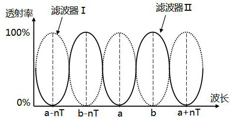
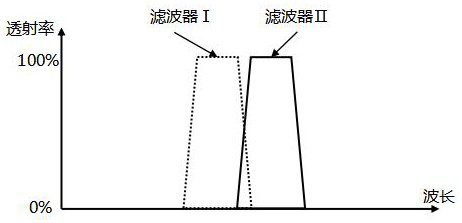
[0083] Among them, the filtering element is composed of two parallel-arranged filter I and filter II;
[0084] The PLC chip provided in this embodiment, by controlling th...
Embodiment 2
[0088] A kind of planar optical waveguide PLC chip, see Figure 4 As shown, including transmitting port, filter element, receiving port and common port;
[0089] The transmitting port communicates with the filter element through an optical transmission channel I, and an optical switch unit I is arranged on the optical transmission channel I;
[0090] The filter element communicates with the receiving port through an optical transmission channel II, and an optical switch unit II is arranged on the optical transmission channel II;
[0091] The filter element communicates with the common port through an optical transmission channel III, and an optical switch unit III is arranged on the optical transmission channel III;
[0092] The transmitting port is used to receive the optical signal emitted by the laser;
[0093] Wherein, the filter element is composed of filter I, filter II and filter III arranged in parallel;
[0094] In the PLC chip provided in this embodiment, by contr...
Embodiment 3
[0106] Set the receiving photodetector (Rx PD), the first monitoring photodetector (MPD1) and the second monitoring photodetector (MPD2) on the surface of the PLC chip (PLC), see Figure 6 As shown, the PLC chip passes the internal etching mirror, and the optical signal enters the receiving photodetector (Rx PD), the first monitoring photodetector (MPD1) and the second monitoring photodetector (MPD2) through reflection;
[0107] see Figure 6 As shown, the top view of the single-fiber bidirectional optical component packaging method 1 with integrated PLC, and see Figure 9 As shown, the side view of the single-fiber bidirectional optical component packaging method 1 with integrated PLC;
[0108] Mount the transimpedance amplifier (TIA) on the PCB / ceramic substrate;
[0109] The receiving photodetector (Rx PD), the first monitoring photodetector (MPD1) and the second monitoring photodetector (MPD2) are mounted on the surface of the PLC chip (PLC) to receive the signal reflect...
PUM
 Abstract
Description
Claims
Application Information
 - R&D Engineer
- R&D Manager
- IP Professional
- Industry Leading Data Capabilities
- Powerful AI technology
- Patent DNA Extraction
Browse by: Latest US Patents, China's latest patents, Technical Efficacy Thesaurus, Application Domain, Technology Topic, Popular Technical Reports.
© 2024 PatSnap. All rights reserved.Legal|Privacy policy|Modern Slavery Act Transparency Statement|Sitemap|About US| Contact US: help@patsnap.com