Method for realizing tunable electromagnetic induction transparency based on graphene-medium composite metasurface
An electromagnetic induction transparent, graphene technology, applied in electrical components, antennas, instruments, etc., can solve the problem of low transmittance and quality factors of EIT windows, and achieve the effect of excellent electromagnetic performance and high transmittance
- Summary
- Abstract
- Description
- Claims
- Application Information
AI Technical Summary
Problems solved by technology
Method used
Image
Examples
Embodiment approach 1
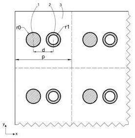
[0033] Embodiment 1: In this embodiment, a feasible and excellent embodiment obtained after design and optimization by the electromagnetic simulation software CST is: p=1500nm, d=530nm, r0=190nm, r1=130nm, h=190nm. The substrate material is quartz, with a dielectric constant of 2.19. The material of the cylindrical nanocolumn and the hollow cylindrical nanocolumn is silicon, and the dielectric constant is 14. The graphene layer selects single-layer graphene. When the above conditions are fixed, the best results can be obtained when the Fermi level is adjusted to 0.6 eV. Figure 5 As shown in (Embodiment 1), when the wavelength of the incident wave changes, an obvious electromagnetic induction transparent window can be observed, and the maximum transmittance reaches 98%.
Embodiment approach 2
[0034]Embodiment 2: In the case of changing the materials of the dielectric substrate and / or the cylindrical and hollow cylindrical structures, the obvious EIT electromagnetic induction transparent window can still be observed in this embodiment. For example, on the basis of Embodiment 1, the material of the dielectric substrate is changed to sapphire with a dielectric constant of 3.1, the material of the cylindrical and hollow cylindrical structures is changed to gallium arsenide with a dielectric constant of 12.9, and in a certain Adjust the size parameters within the range, adjust the Fermi level to 0.6ev, and the transmittance curve spectrum from 1370 nm to 1470 nm can be observed as Figure 5 As shown in (Embodiment 2), the electromagnetic induction transparent window still exists, and the maximum transmittance reaches 97%, which also has the characteristics of high transmittance and high quality factor. This feature will reduce the processing difficulty of related device...
PUM
| Property | Measurement | Unit |
|---|---|---|
| thickness | aaaaa | aaaaa |
| radius | aaaaa | aaaaa |
| radius | aaaaa | aaaaa |
Abstract
Description
Claims
Application Information
 - R&D
- Intellectual Property
- Life Sciences
- Materials
- Tech Scout
- Unparalleled Data Quality
- Higher Quality Content
- 60% Fewer Hallucinations
Browse by: Latest US Patents, China's latest patents, Technical Efficacy Thesaurus, Application Domain, Technology Topic, Popular Technical Reports.
© 2025 PatSnap. All rights reserved.Legal|Privacy policy|Modern Slavery Act Transparency Statement|Sitemap|About US| Contact US: help@patsnap.com


